GENESIS Technical Overview
CONFIDENTIAL
PROPERTY OF SEGA
68000 @8 MHz
- main CPU
- 1 MByte (8 Mbit) ROM Area
- 64 KByte RAM Area
VDP (Video Display Processor)
- dedicated video display processor
- controls playfield & sprites
- capable of DMA
- Horizontal & Vertical interrupts
- 64 KBytes of dedicated VRAM (Video Ram)
- 64 x 9-bits of CRAM (Color RAM)
Z80 @4 MHz
- controls PSG (Programmable Sound Generator) & FM Chips
- 8 KBytes of dedicated Sound Ram
VIDEO:
- NOTE: Playfield and Sprites are character-based
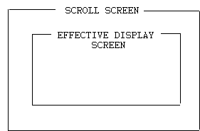
- Display Area (visual)
- 40 chars wide x 28 chars high
- each char is 8 x 8 pixels
- pixel resolution = 320 x 224
- 3 Planes
- 2 scrolling playfields
- 1 sprite plane
- definable priorities between planes
- Playfields:
- 6 different sizes
- 1 playfield can have a "fixed" window
- playfield map
- each char position takes 2 Bytes, that includes:
- char name (10 bits); points to char definition
- horizontal flip
- vertical flip
- color palette (2 bits); index into CRAM
- priority
- each char position takes 2 Bytes, that includes:
- scrolling:
- 1 pixel scrolling resolution
- horizontal:
- whole playfield as unit
- each character line
- each scan line
- vertical:
- whole playfield as unit
- 2 char wide columns
- Sprites:
- 1 x 1 char up to 4 x 4 chars
- up to 80 sprites can be defined
- up to 20 sprites displayed on a scan line
- sprite priorities
- Character Definitions
- 4 bits/pixel; points to color register
- 4 bytes/scanline of char
- 32 bytes for complete char definition
- playfield & sprite chars are the same!
- 40 chars wide x 28 chars high
COLOR:
- Uses CRAM (part of the VDP)
- 64 9-bit wide color registers
- 3 bits of Red
- 3 bits of Green
- 3 bits of Blue
- 4 palettes of 16 colors
- 0th color (of each palette) is always transparent
- 64 9-bit wide color registers
OTHER:
- DMA
- removes the 68000 from the BUS
- can move 205 Bytes/scanline during VBLANK
- there are 36 scanlines during VBLANK
- DMA can move 7380 Bytes during VBLANK
- Horizontal & Vertical interrupts
SOUND:
- Z80 controls:
- PSG (TI 76489 chip)
- FM chip (Yamaha YM 2612)
- 6-channel stereo
- Z80 can access ROM data
- 8 KBytes RAM
HARDWARE:
- 2 controllers
- joypad
- 3 buttons
- Start button
- 1 external port
- 2 video-outs (RF & RGB)
- audio jack
- volume control (for audio jack)
******* INDEX *******
- 1. MEMORY MAP
- § 1 MEGA DRIVE 16BIT MODE
- 68000 MEMORY MAP
- Z80 MEMORY MAP
- 68000 ACCESS TO Z80 MEMORY
- I/O AREA
- CONTROL AREA
- VDP AREA
- Z80 MEMORY MAP
- 2. VDP 315-5313 (Video Display Processor)
- TERMINOLOGY
- § 1 DISPLAY SPECIFICATION
- § 2 VDP STRUCTURE
- § 1 DISPLAY SPECIFICATION
- CTRL
- VRAM
- CRAM
- VSRAM
- DMA
- VRAM
- § 3 INTERRUPTS
- VERTICAL INTERRUPT
- HORIZONTAL INTERRUPT
- EXTERNAL INTERRUPT
- HORIZONTAL INTERRUPT
- § 4 VDP INTERFACE
- $C00000 (DATA CHANNEL)
- $C00004 (CONTROL CHANNEL)
- $C00008 (HV COUNTER)
- $C00004 (CONTROL CHANNEL)
- § 5 VDP REGISTER
- Reg. # 0 - Reg. # 3
- Reg. # 4 - Reg. #10
- Reg. #11 - Reg. #14
- Reg. #15 - Reg. #18
- Reg. #19 - Reg. #23
- Reg. # 4 - Reg. #10
- § 6 ACCESS VDP RAM
- ADDRESS SETTING
- VRAM ACCESS
- CRAM ACCESS
- VSRAM ACCESS
- ACCESS TIMING
- HV COUNTER
- VRAM ACCESS
- § 7 DMA
- MEMORY TO VRAM
- VRAM FILL
- VRAM COPY
- DMA ABILITY
- VRAM FILL
- § 8 SCROLL
- SCREEN SIZE
- HORIZONTAL SCROLL
- VERTICAL SCROLL
- SCROLL PATTERN
- PATTERN NAME
- HORIZONTAL SCROLL
- § 9 WINDOW
- POSITION
- PRIORITY
- PATTERN NAME
- PRIORITY
- § 10 SPRIT_E
- POSITION
- ATTRIBUTE
- SIZE
- ABILITY
- PRIORITY (SPRITES)
- PATTERN GENERATOR
- ATTRIBUTE
- § 11 PRIORITY
- § 12 COLOR PALETTE
- § 13 INTERLACE MODE
- § 12 COLOR PALETTE
- 3. 8/16 BIT COMPATIBILITY
- MARK III (MS - JAPAN)
- MS
- RAM CARD
- MS
- 4. I/O
- § 1 VERSION NO.
- § 2 I/O
- § 3 MEMORY MODE
- § 4 Z80 CONTROLS
- § 2 I/O
- Z80 BUSREQ
- Z80 RESET
- § 5 Z80 AREA
- SOUND RAM
- SOUND CHIP
- BANK REGISTER
- SOUND CHIP
- 5. VRAM MAPPING
- 6. APPEND
1. MEMORY MAP
§ 1 MEGA DRIVE 16 BIT MODE (AS DISTINCT FROM MASTER SYSTEM COMPATIBILITY MODE)
_ 68K MEMORY MAP _

_ Z80 MEMORY MAP _
_ 68000 ACCESS TO Z80 MEMORY _
_ I/O AREA _
_ CONTROL AREA _
_ VDP AREA _

2. VDP 315 - 5313
(Video Display Processor)
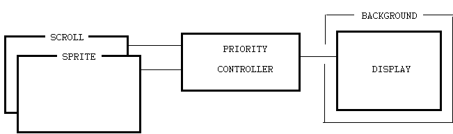
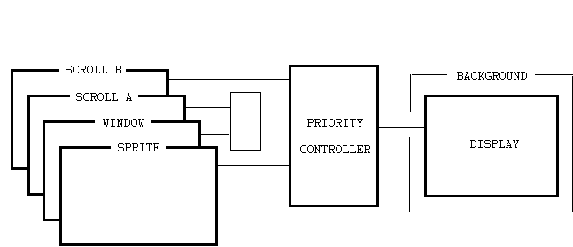
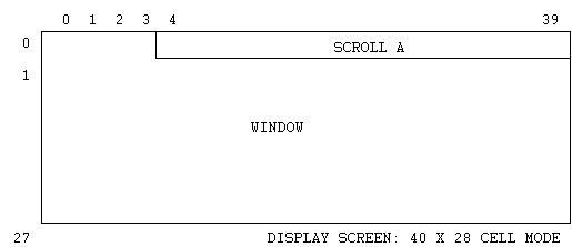
The VDP controls screen display. VDP has graphic modes IV and V. Where Mode IV is for compatibility with the MASTER SYSTEM and V is for the new Mega drive functions. There are no advantages to using mode IV. so it is assumed that all Mega drive development will use mode V. In Mode V. the VDP display has 4 planes: SPRITE, SCROLL A/WINDOW, SCROLL B, and BACKGROUND.
GRAPHIC IV MODE (COMPATIBILITY MODE)
GRAPHIC V MODE (16 BIT MODE)
_ TERMINOLOGY _
1. A unit of Position on X Y coordinates is called a "DOT".
2. A minimum unit of display is called a "PIXEL".
3. "CELL" means an 8 (pixel) x 8 (pixel) pattern.
4. SCROLL indicated a repositionable screen-spanning play field.
5. CPU usually indicates the 68000.
6. VDP stands for Video Display Processor.
7. CTRL stands for Control.
8. VRAM stands for VDP RAM, the 64K bytes area of RAM accessible only through the VDP.
9. CRAM stands for Color RAM, 64 9 bit words inside the VDP chip.
10. VSRAM stands for vertical Scroll RAM. 40 10-bit words inside the VDP chip.
11. DMA stands for Direct Memory Access, the process by which the VDP performs high speed fills or memory copies.
12. PSG stands for Programmable sound Generator. A class of low-capability Sound chips. The Mega drive contains a Texas Instruments 76489 PSG chip.
13. FM stands for Frequency Modulation, a class of high-capability sound chip. The Mega drive contains a Yamaha 2612 FM chip.
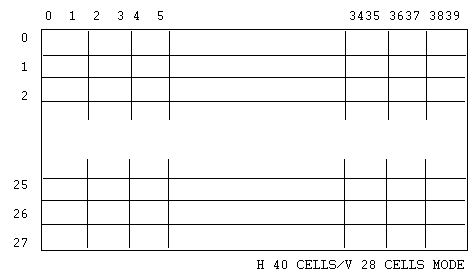
§ 1 DISPLAY SPECIFICATION
DISPLAY SPECIFICATION OUTLINE
| DISPLAY SIZE | THERE ARE TWO MODES:
32*28 CELL (256*224 PIXEL)
|
| CHARACTER GENERATOR | 8*8 CELLS 1300-1800 depending on general system configuration. |
| SCROLL PLAYFIELDS | Two scrolling play fields. whose size in cells is selectable from:
32*32, 32*64, 32*128,
|
| SPRITE | Sprite size is programmable on a sprite by sprite basis. with the following choices:
8*8, 8*16, 8*24, 8*32
There are 64 sprites available when the screen is in 32 cell wide mode. Or 80 when the screen is in 40 cell wide mode. |
| WINDOW | 1 window associated with the Scroll A play field. |
| COLORS | 64 colors/512 possibilities |
For PAL (the European Television 50HZ standard), a vertical size of 30 cells (240 dots) is selectable. The VDP supports both NTSC and PAL television standards. In both cases, the screen is divided into active scan, where the picture is displayed, and vertical retrace (or vertical blanking) where the monitor prepares for the next display.
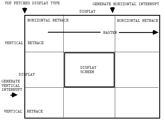
Numbers of rasters in a screen are as follows:
| Lines/Screen | VCELL | LINE NO. (DISPLAY) | LINE NO. (RETRACE) | |
| NTSC | 262 | 28 | 224 RASTER | 38 RASTER |
| PAL | 312 | 28 | 224 RASTER | 98 RASTER |
| PAL | 312 | 30 | 240 RASTER | 82 RASTER |
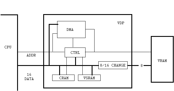
§2 VDP STRUCTURE
The CPU controls the VDP by special I/O memory locations.
_ CTRL (Control) _
This controls REGISTER, VRAM, CRAM, VSRAM, DMA DISPLAY, etc.
_ VRAM (VDP RAM) _
General purpose storage area for display data.
_ CRAM (COLOR RAM) _
64 colors divided into 4 palettes of 16 colors each.
_ VSRAM (Vertical scroll RAM) _
Up to 20 different vertical scroll values each for scrolling play fields A and B.
_ DMA (Direct Memory Access) _
The VDP may move data at high speed from CPU memory to VRAM, CRAM, and VSRAM instead of the CPU, by taking the 68000 off the bus and doing DMA itself. The VDP can also fill the VRAM with a constant, or copy from VRAM to VRAM without disturbing the 68000.
§ 3 INTERRUPT
There are three interrupts: Vertical, Horizontal, and External. You can control each interrupt by the IE0, IE1, and IE2 bits in the VDP registers. The interrupts use the AUTO-VECTOR mode of the 68000 and are at levels 6, 4, and 2 respectively. The level 6 vertical interrupt having the highest priority.
| IE0 | VInterrupt | (LEVEL6) |
| IE1 | HInterrupt | (LEVEL4) |
| IE2 | External Interrupt | (LEVEL2) |
| 1 : Enable | ||
| 0 : Disable |
_ VERTICAL INTERRUPT (V-INT) _
The vertical interrupt occurs just after V retrace.

_ HORIZONTAL INTERRUPT (H-INT) _
The horizontal interrupt occurs just before H retrace.
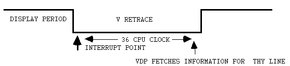
The VDP loads the required display information, including all required register values, for the line in about 36 clocks, thus the CPU can control the display of the next line but not the line on which the interrupt occurs.
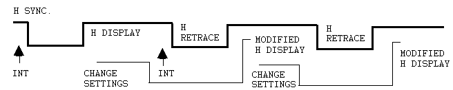
The horizontal interrupt is controlled by a line counter in register #10. If this line counter is changed at each interrupt, the desired spacing of interrupts may be achieved.
| Thus: | If Register #10 equals 00h then the interrupt occurs every line. |
| If Register #10 equals 01h then the interrupt occurs every other line. | |
| If Register #10 equals 02h then the interrupt occurs every third line. |
_ EXTERNAL INTERRUPT (EX-INT) _
The external interrupt is generated by a peripheral device (gun, modem) and stops the counter for later examination by the CPU.

Please see other sections of this manual for information about the H, V counter and the initialization of the external interrupt.
§ 4 VDP PORT
The VDP ports are at location $C00000 in the 68000 memory space.
| UPPER BYTE | LOWER BYTE | |||
| $ C00000 | DATA PORT | ||
| $ C00002 | " | ||
| $ C00004 | CONTROL PORT | ||
| $ C00006 | " | ||
| $ C00008 | HV COUNTER | ||
| $ C0000A | PROHIBITED | ||
| $ C0000C | PROHIBITED | ||
| $ C0000E | PROHIBITED | ||
| $ C00010 | PROHIBITED | PSG | |
_ $ C00000 (DATA PORT) _
READ/WRITE: VRAM, VSRAM, CRAM
| $C00000 | DT15 | DT14 | DT13 | DT12 | DT11 | DT10 | DT9 | DT8 | ( D15 ~ D8 ) | |||||||||||
| DT7 | DT6 | DT5 | DT4 | DT3 | DT2 | DT1 | DT0 | ( D7 ~ D0 ) | ||||||||||||
| * $C00000 and $C00002 are functionally equivalent. | ||||||||||||||||||||
_ $ C00004 (CONTROL PORT) _
READ : STATUS REGISTER
| $C00004 | * | * | * | * | * | * | EMPT | FULL | ( D15 ~ D8 ) | |||||||||||
| F | SOVR | C | ODD | VB | HB | DMA | PAL | ( D7 ~ D0 ) | ||||||||||||
* NO USE
| EMPT | 1: | WRITE FIFO EMPTY |
| 0: | ||
| FUL | 1: | WRITE FIFO FULL |
| 0: | ||
| F | 1: | V interrupt happened. |
| SOVR | 1: | Sprites overflow occurred, too many in one line. |
| Over 17 in 32 cell mode. | ||
| Over 21 in 40 cell mode. | ||
| C | 1: | Collision happened between non-zero pixels in two sprites. |
| 0: | ||
| ODD | 1: | Odd frame in interlace mode. |
| 0: | Even frame in interlace mode. | |
| VB | 1: | During V blanking |
| 0: | ||
| HB | 1: | During H blanking |
| 0: | ||
| DMA | 1: | DMA BUSY |
| 0: | ||
| PAL | 1: | PAL MODE |
| 0: | NTSC MODE |
WRITE1 : REGISTER SET
| $C00004 | 1 | 0 | 0 | RS4 | RS3 | RS2 | RS1 | RS0 | ( D15 ~ D8 ) | |||||||||||
| D7 | D6 | D5 | D4 | D3 | D2 | D1 | D0 | ( D7 ~ D0 ) | ||||||||||||
| * $C00004 and $C00006 are functionally equivalent. | ||||||||||||||||||||
| RS4 ~ RS0 | : Register No. |
| D7 ~ D0 | : Date |
* You must use word or long word access to VDP ports when setting the registers. Long word access is equivalent to two word accesses, with D31-D16 written first.
WRITE2 : ADDRESS SET
| 1st | CD1 | CD0 | A13 | A12 | A11 | A10 | A9 | A8 | ( D15 ~ D8 ) | |||||||||||
| $ C00004 | A7 | A6 | A5 | A4 | A3 | A2 | A1 | A0 | ( D7 ~ D0 ) | |||||||||||
| 2nd | 0 | 0 | 0 | 0 | 0 | 0 | 0 | 0 | ( D15 ~ D8 ) | |||||||||||
| $ C00004 | CD5 | CD4 | CD3 | CD2 | 0 | 0 | A15 | A14 | ( D7 ~ D0 ) | |||||||||||
| CD5 ~ CD0 | : ID CODE |
| A15 ~ A0 | : DESTINATION RAM ADDRESS |
| ACCESS MODE | CD5 | CD4 | CD3 | CD2 | CD1 | CD0 |
| VRAM WRITE | 0 | 0 | 0 | 0 | 0 | 1 |
| CRAM WRITE | 0 | 0 | 0 | 0 | 1 | 1 |
| VSRAM WRITE | 0 | 0 | 0 | 1 | 0 | 1 |
| VRAM READ | 0 | 0 | 0 | 0 | 0 | 0 |
| CRAM READ | 0 | 0 | 1 | 0 | 0 | 0 |
| VSRAM READ | 0 | 0 | 0 | 1 | 0 | 0 |
* You must use word or long word when performing these operations.
_ $ C00008 (HV Counter) _
NON INTERLACE MODE
| $ C00008 | VC7 | VC6 | VC5 | VC4 | VC3 | VC2 | VC1 | VC0 | ( D15 ~ D8 ) | |||||||||||
| HC8 | HC7 | HC6 | HC5 | HC4 | HC3 | HC2 | HC1 | ( D7 ~ D0 ) | ||||||||||||
INTERLACE MODE
| $ C00008 | VC7 | VC6 | VC5 | VC4 | VC3 | VC2 | VC1 | VC8 | ( D15 ~ D8 ) | |||||||||||
| HC8 | HC7 | HC6 | HC5 | HC4 | HC3 | HC2 | HC1 | ( D7 ~ D0 ) | ||||||||||||
| HC8 ~ HC1 | : H COUNTER |
| VC8 ~ VC0 | : V COUNTER |
§ 4 VDP REGISTER
VDP has write only register #0 through #23 and read only status register total 25 register. These are two modes for register settings. One is mode 4 and another is mode 5. We tell you about mode 5 in this section and about mode 4 see MARK section. If you change mode in one frame you can get various effects.
MODE SET REGISTER No. 1
| MSB | LSB | |||||||
| REG. # 0 | 0 | 0 | 0 | IE1 | 0 | 1 | M3 | 0 |
| IE1 | 1: Enable H interrupt (68000 Level 4) |
| 0: Disable H interrupt (REG #10) | |
| M3 | 1: HV. Counter stop |
| 0: Enable read HV. counter |
MODE SET REGISTER No. 2
| MSB | LSB | |||||||
| REG. # 1 | 0 | DISP | IE0 | M1 | M2 | 1 | 0 | 0 |
| DISP | 1: Enable Display |
| 0: Disable Display | |
| IE0 | 1: Enable V interrupt (68000 Level 6) |
| 0: Disable V interrupt | |
| M1 | 1: DMA Enable |
| 0: DMA Disable | |
| M2 | 1: V 30 cell mode (PAL mode) |
| 0: V 28 cell mode (PAL mode, always 0 in NTSC mode) |
PATTERN NAME TABLE BASE ADDRESS FOR SCROLL A
| MSB | LSB | |||||||
| REG. # 2 | 0 | 0 | SA15 | SA14 | SA13 | 0 | 0 | 0 |
VRAM ADDR $XXX0_0000_0000_0000
PATTERN NAME TABLE BASE ADDRESS FOR WINDOW
| MSB | LSB | |||||||
| REG. # 3 | 0 | 0 | WD15 | WD14 | WD13 | WD12 | WD11 | 0 |
WD11 should be 0 in H40 cell mode
VRAM ADDR $ XXXX_X000_0000_0000 (H 32 cell mode)
VRAM ADDR $ XXXX_0000_0000_0000 (H 40 cell mode)
PATTERN NAME TABLE BASE ADDRESS FOR SCROLL B
| MSB | LSB | |||||||
| REG. # 4 | 0 | 0 | 0 | 0 | 0 | SB15 | SB14 | SB13 |
VRAM ADDR $XXX0_0000_0000_0000
SPRITE ATTRIBUTE TABLE BASE ADDRESS
| MSB | LSB | |||||||
| REG. # 5 | 0 | AT15 | AT14 | AT13 | AT12 | AT11 | AT10 | AT9 |
AT9 should be 0 in H 40 cell mode
VRAM ADDR $XXXX_XXX0_0000_0000 ( 32 cell )
VRAM ADDR $XXXX_XX00_0000_0000 ( 40 cell )
| MSB | LSB | |||||||
| REG. # 6 | 0 | 0 | 0 | 0 | 0 | 0 | 0 | 0 |
BACKGROUND COLOR
| MSB | LSB | |||||||
| REG. # 7 | 0 | 0 | CPT1 | CPT0 | COL3 | COL2 | COL1 | COL0 |
CPT1,0 : COLOR PALLET
COL3 ~ 0 : COLOR CODE
| MSB | LSB | |||||||
| REG. # 8 | 0 | 0 | 0 | 0 | 0 | 0 | 0 | 0 |
| MSB | LSB | |||||||
| REG. # 9 | 0 | 0 | 0 | 0 | 0 | 0 | 0 | 0 |
H INTERRUPT REGISTER
| MSB | LSB | |||||||
| REG. # 10 | BIT7 | BIT6 | BIT5 | BIT4 | BIT3 | BIT2 | BIT1 | BIT0 |
This register makes H interrupt timing by number of Raster
H interrupt is enabled by IE=1
MODE SET REGISTER No. 3
| MSB | LSB | |||||||
| REG. # 11 | 0 | 0 | 0 | 0 | IE2 | VSCR | HSCR | LSCR |
IE2 1: Enable external interrupt (68000 Level 2)
0: Disable external interrupt
* See INTERRUPT and SYSTEM I/O
VSCR: V scroll mode HSCR, LSCR: H scroll mode
| VSCR | FUNCTION | HSCR | LSCR | FUNCTION | |
| 0 | FULL SCROLL | 0 | 0 | FULL SCROLL | |
| 1 | EACH 2 CELL SCROLL | 0 | 1 | PROHIBITED | |
| 1 | 0 | EACH 1 CELL SCROLL | |||
| 1 | 1 | EACH 1 LINE SCROLL |
* BOTH SCROLL A AND B
MODE SET REGISTER No. 4
| MSB | LSB | |||||||
| REG. # 12 | RS0 | 0 | 0 | 0 | S/TE | LSM1 | LSM0 | RS1 |
| RS0 | 0: | Horizontal 32 cell mode |
| 1: | Horizontal 40 cell mode | |
| RS1 | 0: | Horizontal 32 cell mode |
| 1: | Horizontal 40 cell mode | |
| * | You should set same No. in RS0, RS1. | |
| 32 cell 0000_XXX0 | ||
| 40 cell 1000_XXX1 | ||
| S/TE | 1: | Enable SHADOW and HIGHLIGHT. |
| 0: | Disable SHADOW and HIGHLIGHT. | |
| LSM1, LSM0 | : | Interlace mode setting |
| LSM1 | LSM0 | FUNCTION |
| 0 | 0 | NO INTERLACE |
| 0 | 1 | INTERLACE |
| 1 | 0 | PROHIBITED |
| 1 | 1 | INTERLACE (Double Resolution) |
H SCROLL DATA TABLE BASE ADDRESS
| MSB | LSB | |||||||
| REG. # 13 | 0 | 0 | HS15 | HS14 | HS13 | HS12 | HS11 | HS10 |
VRAM ADDR $XXXX_XX00_0000_0000
| MSB | LSB | |||||||
| REG. # 14 | 0 | 0 | 0 | 0 | 0 | 0 | 0 | 0 |
AUTO INCREMENT DATA
This register controls bias number of increment data.
| MSB | LSB | |||||||
| REG. # 15 | INC7 | INC6 | INC5 | INC4 | INC3 | INC2 | INC1 | INC0 |
INC7 ~ 0: Bias number ( 0 ~ $FF )
This number is added automatically after ram access.
SCROLL SIZE
| MSB | LSB | |||||||
| REG. # 16 | 0 | 0 | VSZ1 | VSZ0 | 0 | 0 | HSZ1 | HSZ0 |
| VSZ1 | VSZ0 | FUNCTION | HSZ1 | HSZ0 | FUNCTION | |
| 0 | 0 | V 32 cell | 0 | 0 | H 32 cell | |
| 0 | 1 | V 64 cell | 0 | 1 | H 64 cell | |
| 1 | 0 | PROHIBITED | 1 | 0 | PROHIBITED | |
| 1 | 1 | V 128 cell | 1 | 1 | H 128 cell |
* Both of scroll A and B
WINDOW H POSITION
| MSB | LSB | |||||||
| REG. # 17 | RIGT | 0 | 0 | WHP5 | WHP4 | WHP3 | WHP2 | WHP1 |
| RIGT | 0: Window is in left side from base point. | |
| 1: Window is in right side from base point. | ||
| WHP5 ~ 1 | Base pointer | 0=Left Side |
| 1=1 cell right | ||
| 2... | ||
WINDOW V POSITION
| MSB | LSB | |||||||
| REG. # 18 | DOWN | 0 | 0 | WVP4 | WVP3 | WVP2 | WVP1 | WVP0 |
| DOWN | 0: Window is in upper side from base point. | |
| 1: Window is in lower side from base point. | ||
| WVP4 ~ 0 | Base pointer | 0=Upper side |
| 1= 1 cell down | ||
| 2... | ||
DMA LENGTH COUNTER LOW
| MSB | LSB | |||||||
| REG. # 19 | LG7 | LG6 | LG5 | LG4 | LG3 | LG2 | LG1 | LG0 |
DMA LENGTH COUNTER HIGH
| MSB | LSB | |||||||
| REG. # 20 | LG15 | LG14 | LG13 | LG12 | LG11 | LG10 | LG9 | LG8 |
LG15 ~ 0: DMA LENGTH COUNTER
DMA SOURCE ADDRESS LOW
| MSB | LSB | |||||||
| REG. # 21 | SA8 | SA7 | SA6 | SA5 | SA4 | SA3 | SA2 | SA1 |
DMA SOURCE ADDRESS MID
| MSB | LSB | |||||||
| REG. # 22 | SA16 | SA15 | SA14 | SA13 | SA12 | SA11 | SA10 | SA9 |
DMA SOURCE ADDRESS HIGH
| MSB | LSB | |||||||
| REG. # 23 | DMD1 | DMD0 | SA22 | SA21 | SA20 | SA19 | SA18 | SA17 |
SA22 ~ 1 : DMA Source address
DMD1, 0 : DMA MODE
| DMD1 | DMD0 | FUNCTION |
| 0 | SA23 | MEMORY TO VRAM |
| 1 | 0 | VRAM FILL |
| 1 | 1 | VRAM COPY |
§ 6 ACCESS VDP RAM
_ RAM ADDRESS SETTING _
You can access VRAM CRAM and VSRAM after writing 32 bits of control data to $C00004 or $C00006. You have to use word or long word when addressing. If you use long word D31 - D16 is 1st, D15 - D0 2nd.
| 1st | CD1 | CD0 | A13 | A12 | A11 | A10 | A9 | A8 | ( D15 ~ D8 ) | |||||||||||
| $ C00004 | A7 | A6 | A5 | A4 | A3 | A2 | A1 | A0 | ( D7 ~ D0 ) | |||||||||||
| 2nd | 0 | 0 | 0 | 0 | 0 | 0 | 0 | 0 | ( D15 ~ D8 ) | |||||||||||
| $ C00004 | CD5 | CD4 | CD3 | CD2 | 0 | 0 | A15 | A14 | ( D7 ~ D0 ) | |||||||||||
CD5 ~ CD0 : ID CODE
A15 ~ A0 : DESTINATION RAM ADDRESS
| CD5 | CD4 | CD3 | CD2 | CD1 | CD0 | |
| VRAM WRITE | 0 | 0 | 0 | 0 | 0 | 1 |
| CRAM WRITE | 0 | 0 | 0 | 0 | 1 | 1 |
| VSRAM WRITE | 0 | 0 | 0 | 1 | 0 | 1 |
| VRAM READ | 0 | 0 | 0 | 0 | 0 | 0 |
| CRAM READ | 0 | 0 | 1 | 0 | 0 | 0 |
| VSRAM READ | 0 | 0 | 0 | 1 | 0 | 0 |
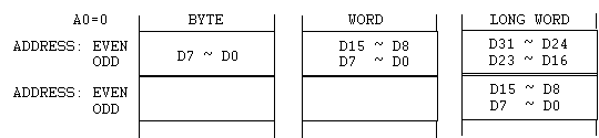
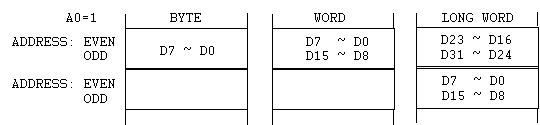
_ VRAM ACCESS _
VRAM address range from 0 to 0FFFFH, 64K bytes total. VRAM access addressing is as follow when writing:
| 1st | 0 | 1 | A13 | A12 | A11 | A10 | A9 | A8 | ( D15 ~ D8 ) | |||||||||||
| $ C00004 | A7 | A6 | A5 | A4 | A3 | A2 | A1 | A0 | ( D7 ~ D0 ) | |||||||||||
| 2nd | 0 | 0 | 0 | 0 | 0 | 0 | 0 | 0 | ( D15 ~ D8 ) | |||||||||||
| $ C00004 | C | 0 | 0 | 0 | 0 | 0 | A15 | A14 | ( D7 ~ D0 ) | |||||||||||
A15 ~ A0 : VRAM address
| Data | D15 | D14 | D13 | D12 | D11 | D10 | D9 | D8 | ( D15 ~ D8 ) | |||||||||||
| $ C00000 | D7 | D6 | D5 | D4 | D3 | D2 | D1 | D0 | ( D7 ~ D0 ) | |||||||||||
D15 ~ D0 : VRAM data
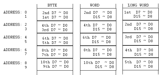
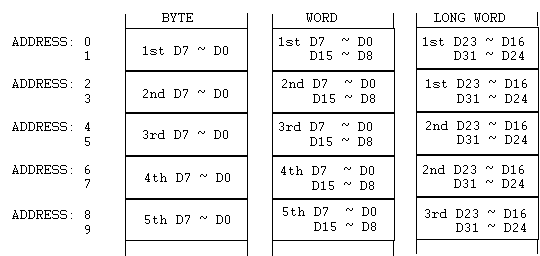
When you use long word D31 ~ D16 is 1st. D15 ~ D0 2nd. When you do byte writing, data is D7 ~ D0, and may be written to $C00000 or $C00001.
VRAM address is increased by the value of REGISTER # 15. independent data size. VRAM address A0 is used in the calculation of the address increment, but is ignored during address decoding.
VRAM addressing and decoding are as follows:
the CRAM address decode uses A15 ~ A1, and A0 specifies the data write format. Write data can not cross a word boundary high and low bytes are exchanged if A0=1.
(EXAMPLE)
START ADDRESS: 0 REG. #15=2
START ADDRESS: 0 REG. #15=1
START ADDRESS: 1 REG. #15=2
START ADDRESS: 1 REG. #15=1
VRAM READ
| 1st | 0 | 0 | A13 | A12 | A11 | A10 | A9 | A8 | ( D15 ~ D8 ) | |||||||||||
| $ C00004 | A7 | A6 | A5 | A4 | A3 | A2 | A1 | A0 | ( D7 ~ D0 ) | |||||||||||
| 2nd | 0 | 0 | 0 | 0 | 0 | 0 | 0 | 0 | ( D15 ~ D8 ) | |||||||||||
| $ C00004 | 0 | 0 | 0 | 0 | 0 | 0 | A15 | A14 | ( D7 ~ D0 ) | |||||||||||
A15 ~ A0 : VRAM address
| Data | D15 | D14 | D13 | D12 | D11 | D10 | D9 | D8 | ( D15 ~ D8 ) | |||||||||||
| $ C00000 | D7 | D6 | D5 | D4 | D3 | D2 | D1 | D0 | ( D7 ~ D0 ) | |||||||||||
D15 ~ D0 : VRAM data
The data is always read in word units. A0 is ignored during the read; no swap of bytes occurs if A0=1. Subsequent reads are from address incremented by REGISTER #15. A0 is used in calculation of the next address.
_ CRAM ACCESS _
The CRAM contains 128 bytes, addresses 0 to 7FH. For word wide writes to the CRAM, use:
| 1st | 1 | 1 | 0 | 0 | 0 | 0 | 0 | 0 | ( D15 ~ D8 ) | |||||||||||
| $ C00004 | 0 | A6 | A5 | A4 | A3 | A2 | A1 | A0 | ( D7 ~ D0 ) | |||||||||||
| 2nd | 0 | 0 | 0 | 0 | 0 | 0 | 0 | 0 | ( D15 ~ D8 ) | |||||||||||
| $ C00004 | 0 | 0 | 0 | 0 | 0 | 0 | 0 | 0 | ( D7 ~ D0 ) | |||||||||||
A6 ~ A0 : VRAM address
| Data | 0 | 0 | 0 | 0 | B2 | B1 | B0 | 0 | ( D15 ~ D8 ) | |||||||||||
| $ C00000 | G2 | G1 | G0 | 0 | R2 | R1 | R0 | 0 | ( D7 ~ D0 ) | |||||||||||
D15 ~ D0 are valid when we use word for data set. If the writes are byte wide, write the high byte to $C00000 and the low byte to $C00001. A long word wide access is equivalent to two sequential word wide accesses. Place the first data in D31 - D16 and the second data in D15 - D0. The data may be written sequentially; the address is incremented by the value of REGISTER #15 after every write, independent of whether the width is byte of word.
Note that A0 is used in the increment but not in address decoding, resulting in some interesting side-effects if writes are attempted at odd addresses.
For word wide reads from the CRAM, use:
| 1st | 0 | 0 | 0 | 0 | 0 | 0 | 0 | 0 | ( D15 ~ D8 ) | |||||||||||
| $ C00004 | 0 | A6 | A5 | A4 | A3 | A2 | A1 | A0 | ( D7 ~ D0 ) | |||||||||||
| 2nd | 0 | 0 | 0 | 0 | 0 | 0 | 0 | 0 | ( D15 ~ D8 ) | |||||||||||
| $ C00004 | 0 | 0 | 1 | 0 | 0 | 0 | 0 | 0 | ( D7 ~ D0 ) | |||||||||||
A6 ~ A0 : VRAM address
| Data | * | * | * | * | B2 | B1 | B0 | * | ( D15 ~ D8 ) | |||||||||||
| $ C00000 | G2 | G1 | G0 | * | R2 | R1 | R0 | * | ( D7 ~ D0 ) | |||||||||||
_ VSRAM ACCESS _
The VSRAM contains 80 bytes, addresses 0 to 4FH. For word wide writes to the VSRAM, use:
| 1st | 0 | 1 | 0 | 0 | 0 | 0 | 0 | 0 | ( D15 ~ D8 ) | |||||||||||
| $ C00004 | 0 | A6 | A5 | A4 | A3 | A2 | A1 | A0 | ( D7 ~ D0 ) | |||||||||||
| 2nd | 0 | 0 | 0 | 0 | 0 | 0 | 0 | 0 | ( D15 ~ D8 ) | |||||||||||
| $ C00004 | 0 | 0 | 0 | 1 | 0 | 0 | 0 | 0 | ( D7 ~ D0 ) | |||||||||||
A6 ~ A0 : VSRAM address
| Data | VS10 | VS9 | VS8 | ( D15 ~ D8 ) | ||||||||||||||||
| $ C00000 | VS7 | VS6 | VS5 | VS4 | VS3 | VS2 | VS1 | VS0 | ( D7 ~ D0 ) | |||||||||||
VS10 - VS0 : V quantity of scroll
If you use word for data and valid in D15 ~ D0. D15 - D0 are valid when we use word for data set. If the writes are byte wide, write the high byte to $C00000 and the low byte to $C00001. A long word wide access is equivalent to two sequential word wide accesses. Place the first data in D31 - D16 and the second data in D15 - D0. The data may be written sequentially; the address is incremented by the value of REGISTER #15 after every write, independent of whether the width is byte of word.
Note that A0 is used in the increment but not in address decoding, resulting in some interesting side-effects if writes are attempted at odd addresses.
For word wide reads from the VSRAM, use:
| 1st | 0 | 0 | 0 | 0 | 0 | 0 | 0 | 0 | ( D15 ~ D8 ) | |||||||||||
| $ C00004 | 0 | A6 | A5 | A4 | A3 | A2 | A1 | A0 | ( D7 ~ D0 ) | |||||||||||
| 2nd | 0 | 0 | 0 | 0 | 0 | 0 | 0 | 0 | ( D15 ~ D8 ) | |||||||||||
| $ C00004 | 0 | 0 | 0 | 1 | 0 | 0 | 0 | 0 | ( D7 ~ D0 ) | |||||||||||
A6 ~ A0 : VSRAM address
| Data | VS10 | VS9 | VS8 | ( D15 ~ D8 ) | ||||||||||||||||
| $ C00000 | VS7 | VS6 | VS5 | VS4 | VS3 | VS2 | VS1 | VS0 | ( D7 ~ D0 ) | |||||||||||
VS10 ~ VS0 : V quantity of scroll
_ ACCESS TIMING _
The CPU and CDP access CRAM, CRAM, and VSRAM using timesharing. Because the VDP is very busy during the active scan, the CPU accesses are limited. However, during vertical blanking the CPU may access the CDP continuously.
The number of permitted accesses by the CPU additionally depends on whether the screen is in 32 cell mode or 40 cell mode. Additionally the access size depends on the RAM type; a VRAM access is byte wide, but CRAM and CSRAM are wor wide.
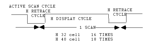

For example, in 32 cell mode, the CPU may access the VRAM 16 times during horizontal scan in a single line. Each access is a byte write, so this amounts to 2 words. However CRAM and CSRAM though sharing the 16 time limit, are word accesses so that 16 words may be written in a single line.
Although there is a four-word FIFO, if writes are done in a tight loop during active scan the FIFO will fill up and the CPU will eventually end up waiting to write.
The maximum wait times are:
| DISPLAY MODE | MAXIMUM WAITING TIME |
| H 32 cell | Approximate 5.96 µsec |
| H 40 cell | Approximate 4.77 µsec |
As the CPU has unlimited access to the RAMs during vertical blanking, the wait case never arises.
_ HV COUNTER _
The HV counter's function is to give the horizontal and vertical location of the television beam. If the "M3" bit of REGISTER #0 is set, the HV counter will then freeze when trigger signal HL goes high, as well as triggering a level 2 interrupt.
| M3 | COUNTER LATCH MODE |
| 0 | COUNTER IS NOT LATCHED BY TRIGGER SIGNAL |
| 1 | COUNTER IS LATCHED BY TRIGGER SIGNAL |
M3: REGISTER # 0
NON INTERLACE MODE
| $ C00008 | VC7 | VC6 | VC5 | VC4 | VC3 | VC2 | VC1 | VC0 | ( D15 ~ D8 ) | |||||||||||
| HC8 | HC7 | HC6 | HC5 | HC4 | HC3 | HC2 | HC1 | ( D7 ~ D0 ) | ||||||||||||
INTERLACE MODE
| $ C00008 | VC7 | VC6 | VC5 | VC4 | VC3 | VC2 | VC1 | VC8 | ( D15 ~ D8 ) | |||||||||||
| HC8 | HC7 | HC6 | HC5 | HC4 | HC3 | HC2 | HC1 | ( D7 ~ D0 ) | ||||||||||||
V-COUNTER : VC7 ~ VC0 H-COUNTER : HC8 ~ HC1
| DISPLAY MODE | COUNTER DATA | DISPLAY MODE | COUNTER DATA | |
| V 28 CELL | 0 ~ DFH | H 32 CELL | 0 ~ 7FH | |
| V 30 CELL | 0 ~ EFH | H 40 CELL | 0 ~ 9FH |
The counter only has eight bits each for H and V, so interlace mode and 40 cell (320 dots) modes present some problems. During interlace mode, the LSB of the vertical position is replaced by the new MSB. And the horizontal resolution problem is solved by ALWAYS dropping the LSB.
CAUTION:
As the HV counter's value is not valid during vertical blanking, check to be sure that it is active scan before using the value.
§ 7 DMA TRANSFER
DMA (Direct Memory Access) is a high speed technique for memory accesses to the VRAM. CRAM and VSRAM. During DMA VRAM, CRAM and VSRAM occur at the fastest possible rate (please see the section on access timing). There are three modes of DMA access. as can be seen below. all of which may be done to VRAM or CRAM or VSRAM. The 68K is stopped during memory to VRAM/CRAM/VSRAM DMA, but the Z80 continues to run as long as it does not attempt access to the 68K memory space.
The DMA is quite fast during VBLANK. about double the tightest possible 68K Top's speed, but during active scan the speed is the same as a 68K loop.
Please note that after this point. VRAM is used as a generic term for VRAM/CRAM/VSRAM.
| DMD1 | DMD0 | DMA MODE | SIZE |
| 0 | SA23 | A. MEMORY TO V-RAM | WORD to BYTE(H)&(L) |
| 1 | 0 | B. VRAM FILL | BYTE to BYTE |
| 1 | 1 | C. VRAM COPY | BYTE to BYTE |
DMD1, DMD0: REG #23 * DMD0=SA23
Source address are $000000-$3FFFFF (ROM) and $FF0000--$FFFFFF (RAM)
for memory to VRAM transfers. In the case of ROM to VRAM transfers, a hardware feature causes occasional failure of DMA unless the following two conditions are observed:
--The destination address write (to address $C00004) must be a word write.
--The final write must use the work RAM.
There are two ways to accomplish this, by copying the DMA program into RAM or by doing a final "move.w ram address $C00004"
_ MEMORY TO VRAM _
The function transfers data from 68K memory to VRAM, CRAM or VSRAM. During this DMA all 68K processing stops. The source address is $000000-$3FFFFF for ROM or $FF0000-$FFFFFF for RAM. The DMA reads are word wide. writes are byte wide for VRAM and word wide for CRAM and VSRAM. The destination is specified by:
| CD2 | CD1 | CD0 | MEMORY TYPE |
| 0 | 0 | 1 | VRAM |
| 0 | 1 | 1 | CRAM |
| 1 | 0 | 1 | VSRAM |
Setting of DMA
(A) M1 (REG. #1)=1 : DMA ENABLE
(B) Increment No. set to #15 (normally 2)
(C) Transfer word No. set into #19, #20.
(D) Source address and DMA mode set into #21, #22, #23.
(E) Set the destination address.
(F)*VDP gets the CPU bus.
(G)*DMA start.
(H)*VDP releases the CPU bus.
(I) M1 have to be 0 after confirmation of DMA finish : DMA DISABLED
DMA starts after (E).
You must set M1=1 only during DMA otherwise we cannot guarantee the operation. Source address were increased with +2 and destination address increased with content of register #15.
Content : of register. Register #1 has another bits.
| MSB | LSB | |||||||
| REG. # 15 | INC7 | INC6 | INC5 | INC4 | INC3 | INC2 | INC1 | INC0 |
INC7 ~ INC0 : No. of increment
| MSB | LSB | |||||||
| REG. # 1 | 0 | DISP | IE0 | M1 | M2 | 1 | 0 | 0 |
| MSB | LSB | |||||||
| REG. # 19 | LG7 | LG6 | LG5 | LG4 | LG3 | LG2 | LG1 | LG0 |
| MSB | LSB | |||||||
| REG. # 20 | LG15 | LG14 | LG13 | LG12 | LG11 | LG10 | LG9 | LG8 |
| MSB | LSB | |||||||
| REG. # 21 | SA8 | SA7 | SA6 | SA5 | SA4 | SA3 | SA2 | SA1 |
| MSB | LSB | |||||||
| REG. # 22 | SA16 | SA15 | SA14 | SA13 | SA12 | SA11 | SA10 | SA9 |
| MSB | LSB | |||||||
| REG. # 23 | DMD1 | DMD0 | SA22 | SA21 | SA20 | SA19 | SA18 | SA17 |
| 1st | CD1 | CD0 | DA13 | DA12 | DA11 | DA10 | DA9 | DA8 | ( D15 ~ D8 ) | |||||||||||
| $ C00004 | A7 | A6 | A5 | A4 | A3 | A2 | A1 | A0 | ( D7 ~ D0 ) | |||||||||||
| 2nd | 0 | 0 | 0 | 0 | 0 | 0 | 0 | 0 | ( D15 ~ D8 ) | |||||||||||
| $ C00004 | 1 | 0 | 0 | CD2 | 0 | 0 | DA15 | DA14 | ( D7 ~ D0 ) | |||||||||||
LG15 - LG0 : No. of move word
SA23 - SA1 : Source address (in 68000)
DA15 - DA0 : Destination address (in VDP)
CD2 - CD0 : RAM selection
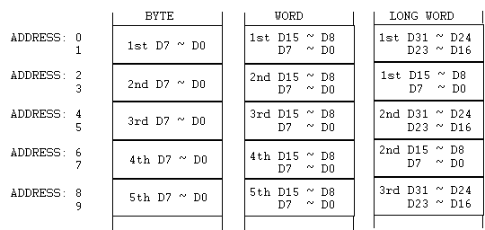
_ VRAM FILL _
FILL mode fills with same data from free even VRAM address.
FILL for only VRAM.
How to set FILL(DMA).
(A) M1 (REG. #1)=1 : DMA ENABLE
(B) Increment No. set to #15 (normally 1).
(C) Fill size set to #19, #20.
(D) DMA mode set to #23.
(E) Destination address and FILL data set.
(F) *DMA start
(G) M1=0 after confirmation of finishing
:DMA DISABLED
DMA starts at after (E).
M1 should be 1 in the DMA transfer. otherwise we can't guarantee the operation. Destination address is incremented with register #15. VDP dose not asks bus open for CPU, but CPU cannot access VDP without PSG. HV counter and status. You can realize end of DMA, by DMA bit in status register.
Register setting. Register #1 has another bits.
| MSB | LSB | |||||||
| REG. # 15 | INC7 | INC6 | INC5 | INC4 | INC3 | INC2 | INC1 | INC0 |
INC7 - INC0 : Increment No.
| STATUS | * | * | * | * | * | * | EMPT | FULL | ||||||||||||
| F | SOVR | C | ODD | DT3 | VB | HB | PAL | |||||||||||||
DMA : 1: DMA BUSY
* : Not care
| MSB | LSB | |||||||
| REG. # 1 | 0 | DISP | IE0 | M1 | M2 | 1 | 0 | 0 |
| MSB | LSB | |||||||
| REG. # 19 | LG7 | LG6 | LG5 | LG4 | LG3 | LG2 | LG1 | LG0 |
| MSB | LSB | |||||||
| REG. # 20 | LG15 | LG14 | LG13 | LG12 | LG11 | LG10 | LG9 | LG8 |
| MSB | LSB | |||||||
| REG. # 23 | DMD1 | DMD0 | SA22 | SA21 | SA20 | SA19 | SA18 | SA17 |
| 1st | 0 | 1 | DA13 | DA12 | DA11 | DA10 | DA9 | DA8 | ( D15 ~ D8 ) | |||||||||||
| $ C00004 | A7 | A6 | A5 | A4 | A3 | A2 | A1 | A0 | ( D7 ~ D0 ) | |||||||||||
| 2nd | 0 | 0 | 0 | 0 | 0 | 0 | 0 | 0 | ( D15 ~ D8 ) | |||||||||||
| $ C00004 | 1 | 0 | 0 | 0 | 0 | 0 | DA15 | DA14 | ( D7 ~ D0 ) | |||||||||||
| Data | FD15 | FD14 | FD13 | FD12 | FD11 | FD10 | FD9 | FD8 | ( D15 ~ D8 ) | |||||||||||
| $ C00000 | FD7 | FD6 | FD5 | FD4 | FD3 | FD2 | FD1 | FD0 | ( D7 ~ D0 ) | |||||||||||
LG15 - LG0 : FILL byte No.
DA15 - DA0 : Destination address
FD15 - FD0 : FILL date
When setting 1st and 2nd by long word. 1st will be D31 - D16 and 2nd, D15 - D0.
EXAMPLE:
1 TERM: FILL data are word;register #15=1
a. V-RAM address is even.
(A) First, low side of FILL data are written in V-RAM address.
(B) Second, upper side of FILL data are written in V-RAM+1.
(C) And, V-RAM address is added register #15, written upper side
FILL data in V-RAM at next each step.
b. V-RAM address is odd.
(D) First, upper side of Fill data are written in
V-RAM address-1.
(E) Second, low side of Fill data are written in V-RAM.
(F) Same as (C).
•VRAM address is even: •VRAM address is odd;
| ADD | (A) | Even | ADD-1 | (D) | Even | |
| ADD+1 | (B) (C) | Odd | ADD | (E) | Odd | |
| ADD+2 | (C) | ADD+1 | (F) | |||
| ADD+3 | (C) | ADD+2 | (F) | |||
| ADD+4 | (C) | ADD+3 | (F) | |||
| ADD+5 | (C) | ADD+4 | (F) | |||
| ADD+6 | (C) | ADD+5 | (F) | |||
| ADD+7 | ADD+6 | (F) | ||||
| ADD+7 |
* You must rewrite data (C) into ADD+1 after write data (B).
2. TERM: FILL data are word; resister #15=2
•VRAM address=even •VRAM address=odd
| ADD | (A) lower | Even | ADD-1 | (D) upper | Even | |
| ADD+1 | (B) upper | Odd | ADD | (E) lower | Odd | |
| ADD+2 | (C) lower | ADD+1 | ||||
| ADD+3 | upper | ADD+2 | (F) upper | |||
| ADD+4 | (C) lower | ADD+3 | lower | |||
| ADD+5 | upper | ADD+4 | (F) upper | |||
| ADD+6 | (C) lower | ADD+5 | lower | |||
| ADD+7 | upper | ADD+6 | (F) upper | |||
| ADD+7 | lower |
3. TERM: Fill data are byte.
a. V-RAM address is even.
(A) = (B) = (C) = BYTE * DATA
b. V-RAM address is odd.
(D) = (E) = (F) = BYTE * DATA
_ VRAM COPY _
This function dose copy from source address to destination address by number of COPY byte.
DMA setting
(A) M1 (REG. #1) = 1 : DMA ENABLE
(B) Number of copy bytes in #19, #20
(C) Source address and DMA mode in #23.
(D) Destination address set.
(E) *DMA transfer
(F) After confirming DMA finish
:M1=0:DMA DISABLED
DMA starts when (D) above is finished. Apply M1=1 only during DMA transfer. In other cases, if M1=1 is set, there is no guaranty that it will function correctly. At the time of DMA transfer, the destination address is incremented by the set value of REG. #15. During DMA transfer. although the VDP does not require CPU to make a bus available, no access is possible from CPU to VDP except for PSG, HV counter. STATUS READ. DMA transfer finish can be recognized by referring to the STATUS REGISTER's DMA bit.
Example: With TRANSFER BYTE=3 at the time of VRAM COPY
REG#15=1 REG#15=2
SOURCE ADDRESSDESTINATION ADDRESS DESTINATION ADDRESS
| DATA 1 | DATA 1 | DATA 1 | ||
| DATA 2 | DATA 2 | |||
| DATA 3 | DATA 3 | DATA 2 | ||
| DATA 4 | ||||
| DATA 5 | DATA 3 | |||
| DATA 6 | ||||
| DATA 7 | ||||
* CAUTION
In the case of VRAM COPY, "read from VRAM" and "write to VRAM" are repeated per byte. Therefore, when the SOURCE AREA and TRANSFER AREA are overlapped, the transfer may not be performed correctly.
The attenuators are set for the four channels by writing the following bytes to I/O location $7F:
| Tone Generator #1: | 1 | 0 | 0 | 1 | A3 | A2 | A1 | A0 |
| Tone Generator #2: | 1 | 0 | 1 | 1 | A3 | A2 | A1 | A0 |
| Tone Generator #3: | 1 | 1 | 0 | 1 | A3 | A2 | A1 | A0 |
| Noise Generator: | 1 | 1 | 1 | 1 | A3 | A2 | A1 | A0 |
EXAMPLE
..When the Mk3 is powered on, the following code is executed:
       LD     HL,CLRTB    ; clear table
       LD     C,PSG_PRT   ; psg port is $7F
       LD     B,4         ; load four bytes
       OTIR               ; write them

       (etc.)

CLTB   defb $9F,$BF,$DF,$FF
This code turns the four sound channels off. It's a good idea to also execute this code when the PAUSE button is pressed, so that the sound does not stay on continuously for the pause interval.
REGISTER are as follows. REGISTER #1 includes bits set for purposes other than DMA. Therefore, pay careful attention in this regard.
| MSB | LSB | |||||||
| REG. # 15 | INC7 | INC6 | INC5 | INC4 | INC3 | INC2 | INC1 | INC0 |
INC7 ~ INC0 : Increment No.
| STATUS | * | * | * | * | * | * | EMPT | FULL | ||||||||||||
| F | SOVR | C | ODD | DT3 | VB | HB | PAL | |||||||||||||
DMA : 1: DMA BUSY
| MSB | LSB | |||||||
| REG. # 1 | 0 | DISP | IE0 | M1 | M2 | 1 | 0 | 0 |
| MSB | LSB | |||||||
| REG. # 19 | LG7 | LG6 | LG5 | LG4 | LG3 | LG2 | LG1 | LG0 |
| MSB | LSB | |||||||
| REG. # 20 | LG15 | LG14 | LG13 | LG12 | LG11 | LG10 | LG9 | LG8 |
| MSB | LSB | |||||||
| REG. # 21 | SA7 | SA6 | SA5 | SA4 | SA3 | SA2 | SA1 | SA0 |
| MSB | LSB | |||||||
| REG. # 22 | SA15 | SA14 | SA13 | SA12 | SA11 | SA10 | SA9 | SA8 |
| MSB | LSB | |||||||
| REG. # 23 | 1 | 1 | 0 | 0 | 0 | 0 | 0 | 0 |
| 1st | 0 | 0 | DA13 | DA12 | DA11 | DA10 | DA9 | DA8 | ( D15 ~ D8 ) | |||||||||||
| $ C00004 | DA7 | DA6 | DA5 | DA4 | DA3 | DA2 | DA1 | DA0 | ( D7 ~ D0 ) | |||||||||||
| 2nd | 0 | 0 | 0 | 0 | 0 | 0 | 0 | 0 | ( D15 ~ D8 ) | |||||||||||
| $ C00004 | 1 | 1 | 0 | 0 | 0 | 0 | DA15 | DA14 | ( D7 ~ D0 ) | |||||||||||
LG15 - LG0 : Number of copy byte
SA23 - SA1 : Source address
DA15 - DA0 : Destination address
When setting 1st and 2nd by long word, 1st will be D31 - D16 and 2nd, D15 - D0.
_ DMA TRANSFER CAPACITY _
Transfer quantity varies depending on the DISPLAY MODE as follows:
| DMA MODE | DISPLAY MODE | SCREEN SCANNING | TRANSFER BYTES PER LINE |
| MEMORY | H32 CELL | DURING EFFECTIVE SCREEN DURING V BLANK | 16 Bytes 167 Bytes |
| TO VRAM | H40 CELL | DURING EFFECTIVE SCREEN DURING V BLANK | 18 Bytes 205 Bytes |
| VRAM FILL | H32 CELL | DURING EFFECTIVE SCREEN DURING V BLANK | 15 Bytes 166 Bytes |
| H40 CELL | DURING EFFECTIVE SCREEN DURING V BLANK | 17 Bytes 204 Bytes | |
| VRAM COPY | H32 CELL | DURING EFFECTIVE SCREEN DURING V BLANK | 8 Bytes 83 Bytes |
| H40 CELL | DURING EFFECTIVE SCREEN DURING V BLANK | 9 Bytes 102 Bytes |
In the MEMORY TO VRAM. in the case where CRAM and VSRAM are the destinations, number of words (not byte) should apply. One line during V BLANK allows for data transfer to all the address of CRAM and VSRAM.
Note that when calculating, the transfer quantity in one screen (1/60 sec) varies depending on the number of LINES during V BLANK (refer to DISPLAY MODE) in the case of NTSC (video signal) and PAL systems.
| DISPLAY MODE | No. of Horizontal lines |
| V 28 CELL (NTSC) | 36 |
| V 28 CELL (PAL) | 87 |
| V 30 CELL (PAL) | 71 |
Where REGISTER #1 DISP=0, 1, e.. when on-screen display is not made, the TRANSFER quantity is the same as TRANSFER BYTES PER LINE during BLANKING.
§8 SCROLLING SCREEN
There are two different scroll screens, i.e. A and B which separately can scroll vertically and horizontally on a basis of a one dot unit. In the horizontal direction, scrolling overall or based on a one cell unit or one line unit can be selected. And in the vertical direction. scrolling overall or in. a two cell unit can be selected. Also, the scroll screen size can be changed on a basis of a 32 cell unit.
For the scrolling screen display, the following REGISTER setting and VRAM area are required.
SCROLL "A" PATTERN NAME TABLE BASE ADDRESS
| MSB | LSB | |||||||
| REG. # 2 | 0 | 0 | SA15 | SA14 | SA13 | 0 | 0 | 0 |
SCROLL "B" PATTERN NAME TABLE BASE ADDRESS
| MSB | LSB | |||||||
| REG. # 4 | 0 | 0 | 0 | 0 | 0 | SB15 | SB14 | SB13 |
MODE SET REGISTER No. 3
| MSB | LSB | |||||||
| REG. # 11 | 0 | 0 | 0 | 0 | IE2 | VSCR | HSCR | LSCR |
MODE SET REGISTER No. 4
| MSB | LSB | |||||||
| REG. # 12 | RS0 | 0 | 0 | 0 | S/TE | LSM1 | LSM0 | RS1 |
H SCROLL DATA TABLE BASE ADDRESS
| MSB | LSB | |||||||
| REG. # 13 | 0 | 0 | HS15 | HS14 | HS13 | HS12 | HS11 | HS10 |
SCROLL SIZE
| MSB | LSB | |||||||
| REG. # 16 | 0 | 0 | VSZ1 | VSZ0 | 0 | 0 | HSZ1 | HSZ0 |
| VRAM | : | SCROLL "A" PATTERN NAME TABLE | Max 8K Byte |
| SCROLL "B" PATTERN NAME TABLE | Max 8K Byte | ||
| H SCROLL DATA TABLE | Max 960 Byte | ||
| VSRAM | : | V SCROLL DATA TABLE | Max 80 Byte |
_ SCROLLING SCREEN SIZE _
The screen size can be set by VSZ1, VSZ0, HSZ1, and HSZ0 (REG. #16).
The following 6 kinds can be set both for SCROLL SCREEN A and B.
32*32/32*64/32*128
64*32/64*64
128*32
| VSZ1 | VSC0 | FUNCTION | HSZ1 | HSZ0 | FUNCTION | |
| 0 | 0 | V 32 CELL | 0 | 0 | H 32 CELL | |
| 0 | 1 | V 64 CELL | 0 | 1 | H 64 CELL | |
| 1 | 0 | PROHIBITED | 1 | 0 | PROHIBITED | |
| 1 | 1 | V 128 CELL | 1 | 1 | H 128 CELL |
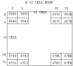
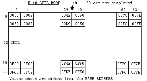
SCROLL SCREEN's PATTERN NAME TABLE ADDRESS exits in the VRAM and is designated by REGISTER #2 and #4. Depending VRAM and SCROLL screen correspond to each other differently.
EXAMPLE
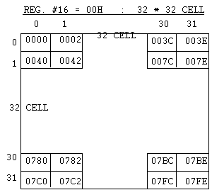
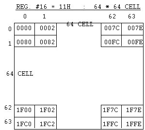
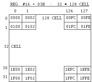
A Value shown in a frame indicates an offset from the PATTERN NAME TABLE BASE ADDRESS.
_ HORIZONTAL SCROLLING _
The DISPLAY SCREEN allows for scrolling overall, or based on one cell unit, or on an dot by dot basis in one line unit. Either one of the above scrolling can be selected by HSCR and LSCR (REGISTER#11). A setting applies to both SCROLL screen A and B.
| HSCR | LSCR | FUNCTION |
| 0 | 0 | OVERALL SCROLLING |
| 0 | 1 | PROHIBITED |
| 1 | 0 | SCROLL IN ONE CELL UNIT |
| 1 | 1 | SCROLL IN ONE LINE UNIT |
HSCR, LSCR: REG. #11
The effective scroll quantity is equivalent to 10 bits (000H-3FFFH).
Taking the DISPLAY SCREEN as standard, the SCROLL direction will be as follows:
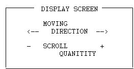
Horizontally scrolling quantity setting area: H Scroll DATA TABLE is in VRAM. From the base address which was set by REG.#13. set the scrolling quantity of SCREEN A and B alternately. Also the scrolling quantity data setting position varies depending on the following mode (OVERALL, 1 CELL. or 1 LINE).
| MODE | SETTING POSITION |
| OVERALL | LINE C |
| 1 CELL | EVERY 8th LINE STARTING FROM LINE 0 |
| 1 LINE | ALL LINES |
| 15 14 13 12 | 11 10 9 8 7 6 5 4 3 2 1 0 | ||
| 00 | A•SCROLLING QUANTITY OF SCREEN A | OVERALL,CELL,LINE | |
| 02 | B•SCROLLING QUANTITY OF SCREEN B | OVERALL,CELL,LINE | |
| 04 | A•SCROLLING QUANTITY OF SCREEN A | LINE | |
| 06 | B•SCROLLING QUANTITY OF SCREEN B | LINE | |
| 08 | A•SCROLLING QUANTITY OF SCREEN A | LINE | |
| 0A | B•SCROLLING QUANTITY OF SCREEN B | LINE | |
|
|
| ||
| 1C | A•SCROLLING QUANTITY OF SCREEN A | LINE | |
| 1E | B•SCROLLING QUANTITY OF SCREEN B | LINE | |
| 20 | A•SCROLLING QUANTITY OF SCREEN A | CELL, LINE | |
| 22 | B•SCROLLING QUANTITY OF SCREEN B | CELL, LINE | |
|
|
| ||
| 3FC | A•SCROLLING QUANTITY OF SCREEN A | LINE | |
| 3FE | B•SCROLLING QUANTITY OF SCREEN B | LINE |
D15 - D10 can be greatly utilized for program software.
_ V SCROLL _
The DISPLAY SCREEN allows for scrolling overall or every 2 Cells in a dot unit. The setting can be done by VSCR (REG.#11). A setting applies to both SCROLL SCREEN A and B.
| VSCR | FUNCTION |
| 0 | OVERALL SCROLL |
| 1 | 2-CELL UNIT SCROLL |
VSCR: REG #11
The scrolling quantity is equivalent to 11 bits (000H--7FFH). However,
it will be as shown below in the INTERLACE MODE.
NON INTERLACE: The effective scrolling quantity is equivalent
to 10 bits.
INTERLACE 1: -ditto-
INTERLACE 2: The effective scrolling quantity
is equivalent to 11 bits.
Taking the DISPLAY SCREEN as standard, the scrolling direction will be
as follows:

Set the V SCROLL quantity by VSRAM. Alternately set the Scroll quantity of SCREEN A and B. Depending on the SCROLL MODE, the DATA setting positions differ.
| MODE | SETTING POSITION |
| OVERALL | ONLY AT THE BEGINNING |
| 2-CELL | SET TO ALL |
| 15 14 13 12 | 11 10 9 8 7 6 5 4 3 2 1 0 | ||
| 00 | A: SCROLL QUANTITY OF SCREEN A | 0,1 CELL,OVERALL | |
| 02 | B: SCROLL QUANTITY OF SCREEN B | 0,1 CELL,OVERALL | |
| 04 | A: SCROLL QUANTITY OF SCREEN A | 2,3 CELL | |
| 06 | B: SCROLL QUANTITY OF SCREEN B | 2,3 CELL | |
| 08 | A: SCROLL QUANTITY OF SCREEN A | 4,5 CELL | |
| 0A | B: SCROLL QUANTITY OF SCREEN B | 4,5 CELL | |
| 0C | A: SCROLL QUANTITY OF SCREEN A | 6,7 CELL | |
| 0E | B: SCROLL QUANTITY OF SCREEN B | 6,7 CELL | |
|
| |||
| 4C | A: SCROLL QUANTITY OF SCREEN A | 38,39 CELL | |
| 4E | B: SCROLL QUANTITY OF SCREEN B | 38,39 CELL |
D15 - D11 is indefinite.
_ SCROLL PATTERN NAME _
The SCROLL SCREEN's name table is in VRAM and set by REG. #2 and #4. The PATTERN NAME requires 2 bytes (1 word) per CELL the SCROLL screen. Depending on the SCROLL screen's size. VRAM and SCROLL SCREEN correspond with each other differently. Refer to SCROLL SCREEN SIZE.
| PATTERN NAME | pri | cp1 | cp0 | vf | hf | pt10 | pt9 | pt8 | ( D15 ~ D8 ) | |||||||||||
| pt7 | pt6 | pt5 | pt4 | pt3 | pt2 | pt1 | pt0 | ( D7 ~ D0 ) | ||||||||||||
| pri | : Refer to PRIORITY |
| cp1 | : Color palette selection hit (See COLOR PALETTE) |
| cp0 | : -ditto- |
| vf | : V REVERSE bit 1: REVERSE |
| hf | : H REVERSE bit 1: REVERSE |
| pt10 - pt0 | : PATTERN GENERATOR NUMBER |
REVERSE BIT vf and hf : Allows for H and V reverse on CELL unit basis.
vf = 0 vf = 1 vf = 0 vf = 1
hf = 0 hf = 0 hf = 1 hf = 1
_ PATTERN GENERATOR _
PATTERN GENERATOR has VRAM 0000H as ,base address, and a pattern is expressed on a 8x8 dot basis. To define a pattern, 32 bytes are required. Starting from 0000H, it proceeds in the sequence of PATTERN GENERATOR O, 1, 2, ... The relationship between the display pattern and memory is as follows:
| 0 | 1 | 2 | 3 | |||||
| D7 | D0 | D7 | D0 | D7 | D0 | D7 | D0 | |
| 00 | a1 | a2 | a3 | a4 | a5 | a6 | a7 | a8 |
| 04 | b1 | b2 | b3 | b4 | b5 | b6 | b7 | b8 |
| 08 | c1 | c2 | c3 | c4 | c5 | c6 | c7 | c8 |
| 0C | d1 | d2 | d3 | d4 | d5 | d6 | d7 | d8 |
| 10 | e1 | e2 | e3 | e4 | e5 | e6 | e7 | e8 |
| 14 | f1 | f2 | f3 | f4 | f5 | f6 | f7 | f8 |
| 18 | g1 | g2 | g3 | g4 | g5 | g6 | g7 | g8 |
| 1C | h1 | h2 | h3 | h4 | h5 | h6 | h7 | h8 |
The display colors and memory relationship is as follows:
| D7 | D6 | D5 | D4 | D3 | D2 | D1 | D0 | |
| COL3 | COL2 | COL1 | COL0 | COL3 | COL2 | COL1 | COL0 |
In INTERLACE MODE 2, one cell consists of 8X16 dots and therefore, 64 Bytes (16 long words) are required.
| 0 | 1 | 2 | 3 | |||||
| D7 | D0 | D7 | D0 | D7 | D0 | D7 | D0 | |
| 00 | a1 | a2 | a3 | a4 | a5 | a6 | a7 | a8 |
| 04 | b1 | b2 | b3 | b4 | b5 | b6 | b7 | b8 |
| 08 | c1 | c2 | c3 | c4 | c5 | c6 | c7 | c8 |
| 0C | d1 | d2 | d3 | d4 | d5 | d6 | d7 | d8 |
| 10 | e1 | e2 | e3 | e4 | e5 | e6 | e7 | e8 |
| 14 | f1 | f2 | f3 | f4 | f5 | f6 | f7 | f8 |
| 18 | g1 | g2 | g3 | g4 | g5 | g6 | g7 | g8 |
| 1C | h1 | h2 | h3 | h4 | h5 | h6 | h7 | h8 |
| 20 | i1 | i2 | i3 | i4 | i5 | i6 | i7 | i8 |
| 24 | j1 | j2 | j3 | j4 | j5 | j6 | j7 | j8 |
| 28 | k1 | k2 | k3 | k4 | k5 | k6 | k7 | k8 |
| 2C | l1 | l2 | l3 | l4 | l5 | l6 | l7 | l8 |
| 30 | m1 | m2 | m3 | m4 | m5 | m6 | m7 | m8 |
| 34 | n1 | n2 | n3 | n4 | n5 | n6 | n7 | n8 |
| 38 | o1 | o2 | o3 | o4 | o5 | o6 | o7 | o8 |
| 3C | p1 | p2 | p3 | p4 | p5 | p6 | p7 | p8 |
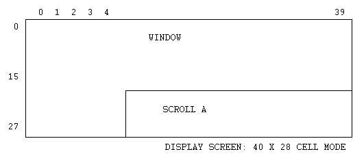
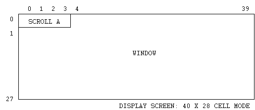
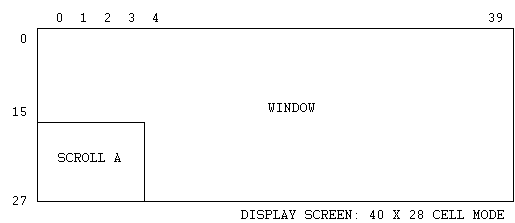
§ WINDOW
For WINDOW display, the following register setting and VRAM areas are required.
WINDOW PATTERN NAME TABLE AND BASE ADDRESS
| MSB | LSB | |||||||
| REG. # 3 | 0 | 0 | WD15 | WD14 | WD13 | WD12 | WD11 | 0 |
MODE SET REGISTER No. 4
| MSB | LSB | |||||||
| REG. # 12 | RS0 | 0 | 0 | 0 | S/TE | LSM1 | LSM0 | RS1 |
WINDOW H POSITION
| MSB | LSB | |||||||
| REG. # 17 | RIGT | 0 | 0 | WHP5 | WHP4 | WHP3 | WHP2 | WHP1 |
WINDOW V POSITION
| MSB | LSB | |||||||
| REG. # 18 | DOWN | 0 | 0 | WVP4 | WVP3 | WVP2 | WVP1 | WVP0 |
VRAM: WINDOW PATTERN NAME TABLE MAX 4K BYTES
_ DISPLAY POSITION _
The WINDOW DISPLAY POSITION is designated by REG #17 and #18.
Screen display can be divided on a unit basis of H 2 cells and V 1 cell. The dividing position varies depending on resolution.
| MSB | LSB | |||||||
| REG. # 17 | RIGT | 0 | 0 | WHP5 | WHP4 | WHP3 | WHP2 | WHP1 |
| MSB | LSB | |||||||
| REG. # 18 | DOWN | 0 | 0 | WVP4 | WVP3 | WVP2 | WVP1 | WVP0 |
RIGT: 0 Displays WINDOW from the left end to H dividing position.
1 Displays WINDOW from the H dividing position to the right end.
DOWN: 0 Displays WINDOW from the top end to the V dividing position.
1 Displays WINDOW from the V dividing position to the bottom end.
WHP5 - WHP1 : H dividing position
WVP4 - WVP0 : V dividing position
| H RESOLUTION | DIVIDING POSITION(WHP) | V RESOLUTION | DIVIDING POSITION(WHP) | |
| 32 CELL | 0 - 16 (0 - 32 CELL) | 28 CELL | 0 - 28 | |
| 40 CELL | 0 - 20 (0 - 40 CELL) | 30 CELL | 0 - 30 |
SETTING EXAMPLE
REG. #17 : 00H + 01H WINDOW from the left end to the second cell
REG. #18 : 00H + 10H WINDOW from the top end to the 16th cell
REG. #17 : 80H + 02H WINDOW from the left end 4th cell to the right end.
REG. #18 : 80H + 01H WINDOW from the 2nd cell to the bottom end
REG. #17 : 80H + 01H WINDOW from the 4th cell to the right end.
REG. #18 : 00H + 10H WINDOW from the top end to the 16th cell.
REG. #17 : 00H + 02H WINDOW to the 4th cell from the left.
REG. #18 : 80H + 01H WINDOW from the 2nd cell to the bottom end.
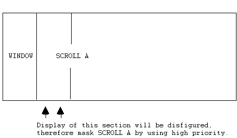
_ WINDOW PRIORITY _
WINDOW PRIORITY is handled in the same way as in SCROLL A. SCROLL A is not displayed in the area where WINDOW is displayed. Also, only when WINDOW is set to the left and SCROLL A is moved in H direction, the character corresponding to 2 cells on the right side of the boundary between WINDOW and SCROLL A will be disfigured. There will be no malfunctioning when the WINDOW is set to the left side and SCROLL A is moved only in V direction. and also when WINDOW is set to the right side.
_ WINDOW PATTERN NAME _
WINDOW PATTERN NAME TABLE is on VRAM, and the BASE ADDRESS is designated by REG. #13. The PATTERN NAME, the same as in SCROLL SCREEN, requires 2 bytes ( 1 Word ) per cell.
| PATTERN NAME | pri | cp1 | cp0 | vf | hf | pt10 | pt9 | pt8 | ( D15 ~ D8 ) | |||||||||||
| pt7 | pt6 | pt5 | pt4 | pt3 | pt2 | pt1 | pt0 | ( D7 ~ D0 ) | ||||||||||||
| pri | : Refer to PRIORITY |
| cp1 | : Color palette selection hit (See COLOR PALETTE) |
| cp0 | : -ditto- |
| vf | : V REVERSE bit 1: REVERSE |
| hf | : H REVERSE bit 1: REVERSE |
| pt10 - pt0 | : PATTERN GENERATOR NUMBER |
PATTERN NAME and VRAM relation varies depending on H 32 cell/40 cell mode. Pay careful attention to this point.
In the H 40 cell mode, there exists the area for H 64 cells. However, there will be no display from the 41st cell in the H direction. Also in the V 28 cell mode, there will be no display from V 29th cell and in the 30th cell mode. There will be no display from 31st cell.
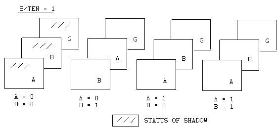
S/TEN = 1
SPRITE COLOR PALETTE 3 COLOR CODE 14


The dots of SPRITE COLOR CODE 15 work as an operator on the screen, the priority of which is lower than SPRITE. Since SPRITE dots work as an operator, this will not be displayed. When SPRITE is not related to PRIORITY, the following PRIORITY applies.

SETTING EXAMPLE
| LINK DATA | |||
| SPRITE 0 | 2 | SPRITE 0 | |
| SPRITE 1 | 10 | SPRITE 2 | |
| SPRITE 2 | 1 | SPRITE 1 | |
| SPRITE 3 | 4 | SPRITE 10 | |
| SPRITE 4 | 5 | SPRITE 11 | |
| SPRITE 5 | 15 | SPRITE 13 | |
| SPRITE 6 | — | SPRITE 3 | |
| SPRITE 7 | 0 | SPRITE 4 | |
| SPRITE 8 | — | SPRITE 5 | |
| SPRITE 9 | — | SPRITE 15 | |
| SPRITE 10 | 11 | SPRITE 7 | |
| SPRITE 11 | 13 | ||
| SPRITE 12 | — | ||
| SPRITE 13 | 3 | ||
| SPRITE 14 | — | ||
| SPRITE 15 | 7 | ||
| SPRITE 16 | — | ||
The 11 SPRITEs shown in the DISPLAY PRIORITY are displayed on the screen. SPRITE No. 6, 8, 9, 12, 14, and 16 onward are not displayed because they are not linked with LINK DATA LIST.
_ SPRITE PATTERN GENERATOR _
The SPRITE PATTERN GENERATOR with VRAM 0000H as BASE ADDRESS, expresses one pattern on a basis of 8x8 dots. 32 bytes are required to define one pattern. Every 32 bytes, one pattern is expressed in the sequence of PATTERN GENERATOR 0, 1, 2... The relationship of DISPLAY PATTERN and MEMORY is the same as in PATTERN GENERATOR. Also, SPRITE SIZE and PATTERN GENERATOR relationship is as follows:
|
V 1 cell H 1 cell
|
V 1 cell H 2 cell
|
V 1 cell H 3 cell
|
V 1 cell H 4 cell
| ||||||||||||||||||||||||||||||||||||||||
|
V 2 cell H 1 cell
|
V 2 cell H 2 cell
|
V 2 cell H 3 cell
|
V 2 cell H 4 cell
| ||||||||||||||||||||||||||||||||||||||||
|
V 3 cell H 1 cell
|
V 3 cell H 2 cell
|
V 3 cell H 3 cell
|
V 3 cell H 4 cell
| ||||||||||||||||||||||||||||||||||||||||
|
V 4 cell H 1 cell
|
V 4 cell H 2 cell
|
V 4 cell H 3 cell
|
V 4 cell H 4 cell
|
§ 11 PRIORITY
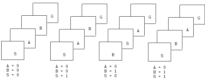
PRIORITY between SPRITE, SCROLL A and SCROLL B can be designated. PRIORITY can be designated by each PATTERN NAME and ATTRIBUTE PRIORITY bit. It will be set for the SCROLL SCREEN on a cell unit basis and for each SPRITE. By combining each priority bit, PRIORITY will be as follows:
However, the BACKGROUND PRIORITY is always the lowest.
| S pri | A pri | B pri | PRIORITY |
| 0 | 0 | 0 | S>A>B>G |
| 1 | 0 | 0 | S>A>B>G |
| 0 | 1 | 0 | A>S>B>G |
| 1 | 1 | 0 | S>A>B>G |
| 0 | 0 | 1 | B>S>A>G |
| 1 | 0 | 1 | S>B>A>G |
| 0 | 1 | 1 | A>B>S>G |
| 1 | 1 | 1 | S>A>B>G |
S : SPRITE
A : SCROLL A
B : SCROLL B
G : BACKGROUND
Also, by combining S/TEN (REG. #12) and the above priority, SHADOW - HIGHLIGHT effect function can be utilized.
S/TEN = 0
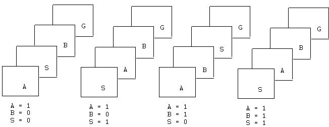
The above shows PRIORITY situation of SPRITE, SCROLL A. SCROLL B and BACKGROUND. The dot to which COLOR CODE 0 is designated is transparent, therefore. either one of SCROLL SCREEN A, B. or BACKGROUND, the priority of which is one step lower than the transparent one, will appear.
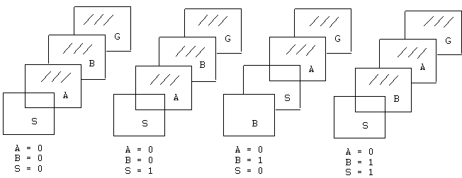
S/TEN = 1
SPRITE COLOR PALETTE 0 - 3 COLOR CODE 0 - 15
COLOR PALETTE 3 COLOR CODE 0 - 13


Where S/TEN=1, when the PRIORITY bit of both SCROLL A and SCROLL B is 0, there will be SHADOW. For the color status, refer to the color palette.
S/TEN = 1
SPRITE COLOR PALETTE 3 COLOR CODE 15
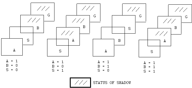
The dots of SPRITE COLOR code 15 work as a SHADOW operator on the screen, the priority of which is lower than the SPRITE. Since SPRITE dots work as an operator, this will not be displayed.
§ INTERLACE MODE
RASTER SCAN MODE can be changed by setting LSM0 and LSM1 (REG. #12).
| LSM1 | LSM0 | RASTER SCAN MODE |
| 0 | 0 | NON INTERLACE MODE |
| 0 | 1 | In the NON-INTERLACE mode, the same PATTERN is displayed on the rasters of even and odd numbered fields.(INTERLACE 1) |
| 1 | 1 | In the INTERLACE mode, the different PATTERN is displayed on the rasters of even and odd numbered fields.(INTERLACE 2) |
In the INTERLACE MODE and INTERLACE 1, one cell is defined by 8x8 dots and in INTERLACE 2, 8x16 dots. For DISPLAY, one cell consists of 8x8 dots in the NON INTERLACE MODE and in the INTERLACE MODE 8x16 dots. In any case, number of cells in one screen are the same. Depending on the type of DISPLAY, in the case of INTERLACE DISPLAY, there may occur a serious blur in the vertical direction. Therefore, when using the DISPLAY pay careful attention in this regard.

3. BACKWARD COMPATIBILITY MODE
In the case of BACKWARD COMPATIBILITY MODE. the MEGA DRIVE differs from the original Mark III & MASTER SYSTEM in the following points:
_ MARK III (MS-JAPAN) _
OS-ROM is not incorporated.
ROM CARTRIDGE/CARD selections are made by hardware in the same manner as in the case of MARK III. START UP SLOT number is not written in 0C000H. START UP Sega logo is not displayed.
FM sound source is not incorporated.
FM sound is incorporated in MS-JAPAN (standard) and MARK III (optional) (OPLL). However, MEGA DRIVE has no option for that, although connection is possible. Consider the MEGA DRIVE's Japanese Specifications as that of MARK III with MS-JAPAN's JOYSTICK Port, or as MS-JAPAN without FM sound source and OS-ROM.
_ MASTER SYSTEM _
OS-ROM is not incorporated.
0C000H-0DFFFH RAM is not clear on POWER-UP.
RAM 0C000 has no meaningful value.
START UP Sega logo not displayed.
FM sound source is not incorporated.
FM sound source is incorporated in MS by option (OPLL). However, MEGA DRIVE has no option, although connection is possible. Please regard the MEGA DRIVE overseas version as a MASTER SYSTEM without an Operating System ROM.
_ RAM BOARD _
In the MEGA DRIVE's MARK III & MASTER SYSTEM BACKWARD COMPATIBILITY MODE, the RAM BOARD for development (for which D-RAM was used) can not be used due to the problem of REFRESH. The other BOARDs for development (which utilizes S-RAM) can be used without any problem.
4. SYSTEM I/O
MEGA DRIVE SYSTEM I/O area assignment starts from $A00000, with the Z80 SUB-CPU's memory area.
§ 1 VERSION NO.
Indicates the Mega Drive's hardware version.
| $A10001 | MODE | VMOD | DISK | RSV | VER3 | VER2 | VER1 | VER0 |
| MODE (R) | 0: Domestic Model |
| 1: Overseas Model | |
| VMOD (R) | 0: NTSC CPU clock 7.67 MHz |
| 1: PAL CPU clock 7.60 MHz | |
| RSV (R) | Currently not used |
| VER3-0 (R) | MEGA DRIVE version is indicated by $0-$F. The present hardware version is indicated by $0. |
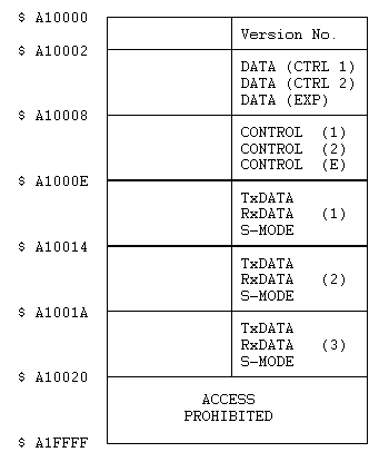
§ 2 I/O PORT
The MEGA DRIVE has the three general purpose I/0 ports, CTRL1, CTRL2 and EXP. Although each port differs from the others in physical shape it functions in the same manner.
Each port has the following S REGISTERs for CONTROL.
| DATA (PARALLEL DATA) | : R/W |
| CTRL (PARALLEL CONTROL) | : R/W |
| S-CTRL (SERIAL CONTROL) | : R/W |
| TxDATA (Txd DATA) | : R/W |
| RxDATA (Rxd DATA) | : R |
The relationship between REGISTERs is as follows:
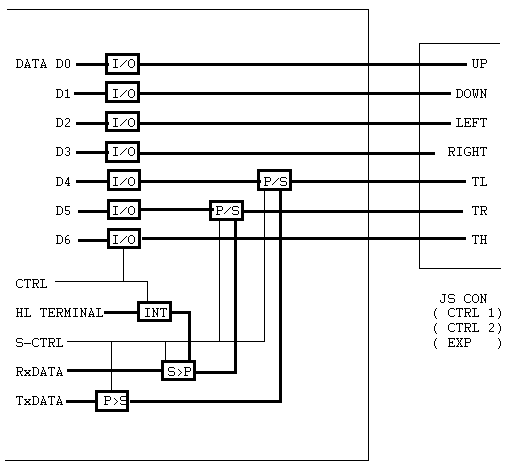
| I/O | : I/O change |
| P/S | : PARALLEL/SERIAL MODE change |
| INT | : INTERRUPT CONTROL |
| S>P | : SERIAL-PARALLEL CONVERSION |
| P>S | : PARALLEL-SERIAL CONVERSION |
Mapping is as follows.
| $A10003 | : DATA 1 ( CTRL1 ) |
| $A10005 | : DATA 2 ( CTRL2 ) |
| $A10007 | : DATA 3 ( EXP ) |
| $A10009 | : CTRL 1 |
| $A1000B | : CTRL 2 |
| $A1000D | : CTRL 3 |
| $A1000F | : TxDATA 1 |
| $A10011 | : RxDATA 1 |
| $A10013 | : S-CTRL 1 |
| $A10015 | : TxDATA 2 |
| $A10017 | : RxDATA 2 |
| $A10019 | : S-CTRL 2 |
| $A1001B | : TxDATA 3 |
| $A1001D | : RxDATA 3 |
| $A1001F | : S-CTRL 3 |
Both BYTE and WORD access are possible. However, in the case of WORD access, only the lower byte is meaningful. DATA shows the status of each port. The I/O direction of each bit is set by CTRL and S-CTRL.
| DATA | PD7 | PD6 | PD5 | PD4 | PD3 | PD2 | PD1 | PD0 |
| PD7 (RW) |
| PD6 (RW) TH |
| PD5 (RW) TR |
| PD4 (RW) TL |
| PD3 (RW) RIGHT |
| PD2 (RW) LEFT |
| PD1 (RW) DOWN |
| PD0 (RW) UP |
CTRL designates the I/O direction of each port and the INTERRUPT CONTROL of TH.
| CTRL | INT | PC6 | PC5 | PC4 | PC3 | PC2 | PC1 | PC0 |
| INT (RW) | 0: TH-INT PROHIBITED |
| 1: TH-INT ALLOWED | |
| PC6 (RW) | 0: PD6 INPUT MODE |
| 1: OUTPUT MODE | |
| PC5 (RW) | 0: PD5 INPUT MODE |
| 1: OUTPUT MODE | |
| PC4 (RW) | 0: PD4 INPUT MODE |
| 1: OUTPUT MODE | |
| PC3 (RW) | 0: PD3 INPUT MODE |
| 1: OUTPUT MODE | |
| PC2 (RW) | 0: PD2 INPUT MODE |
| 1: OUTPUT MODE | |
| PC1 (RW) | 0: PD1 INPUT MODE |
| 1: OUTPUT MODE | |
| PC0 (RW) | 0: PD0 INPUT MODE |
| 1: OUTPUT MODE |
S-CTRL is for the status, etc. of each port's mode change, baud rate and SERIAL.
| S-CTRL | BPS1 | BPS0 | SIN | SOUT | RINT | RERR | RRDY | TFUL |
| SIN (RW) | 0: TR-PARALLEL MODE |
| 1: SERIAL IN | |
| SOUT (RW) | 0: TL-PARALLEL MODE |
| 1: SERIAL OUT | |
| RINT (RW) | 0: Rxd READY INTERRUPT PROHIBITED |
| 1: Rxd READY INTERRUPT ALLOWED | |
| RERR (R) | 0: |
| 1: Rxd ERROR | |
| RRDY (R) | 0: |
| 1: Rxd READY | |
| TFUL (R) | 0: |
| 1: Txd FULL |
| BPS1 | BPS0 | bps |
| 0 | 0 | 4800 |
| 0 | 1 | 2400 |
| 1 | 0 | 1200 |
| 1 | 1 | 300 |
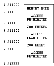
MEMORY MODE
The MEGA DRIVE is able to generate internally the REFRESH signal for the D-RAM development cartridge. When using the development cartridge set to D-RAM MODE. In the case of a production cartridge, set to ROM MODE.
Only D8 of address $A11000 is effective and for WRITE ONLY.
| $A11000 | D8 (W) | 0: ROM MODE |
| 1: D-RAM MODE |
ACCESS to $A11000 can be based on BYTE.
§ 4 Z80 CONTROL
_ Z80 BUSREQ _
When accessing the Z80 memory from the 68000, first stop the Z80 by using BUSREQ. At the time of POWER ON RESET, the 68000 has access to the Z80 bus.
| $A11100 | D8 | (W) | 0: BUSREQ CANCEL |
| 1: BUSREQ REQUEST | |||
| (R) | 0: CPU FUNCTION STOP ACCESSIBLE | ||
| 1: FUNCTIONING |
Access to Z80 AREA in the following manner.
(1) Write $0100 in $A11100 by using a WORD access.
(2) Check to see that D8 of $A11100 becomes 0.
(3) Access to Z80 AREA.
(4) Write $0000 in $A11100 by using a WORD access.
Access to $A11100 can also be based on BYTE.
_ Z80 RESET _
The 68000 may also reset the Z80. The Z80 is automatically reset during the MEGA DRIVE hardware's POWER ON RESET sequence.
| $A11200 | DS (W) | 0: RESET REQUEST |
| 1: RESET CANCEL |
Access to $A11100 can also be based on BYTE.
§5 Z80 AREA
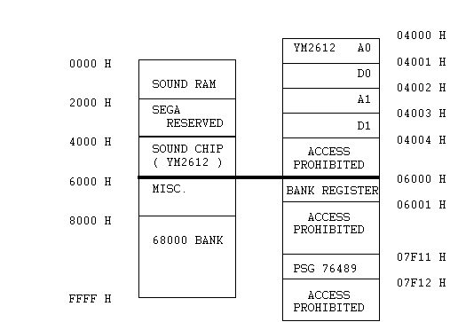
Mapping is performed starting from $A00000 for Z80, a SUB-CPU.
As viewed from 68000. the memory map will be as follows:
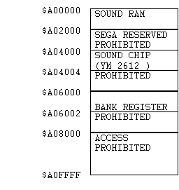
_ SOUND RAM _
This is for the Z80 program. Access from 68000 by BYTE.
_ SOUND CHIP _
This is the mapping area for FM sound source (YM 2612). When accessing from 68000 use BYTE due to timing problem.
_ BANK REGISTER _
Access to the 68000 side MEMORY AREA from Z80 will be based on a 32K BYTE unit. At this time, this REGISTER sets which BANK is to be accessed. Registering from 68000 can be set, however, do not access to Z80 Bank MEMORY AREA by 68000.
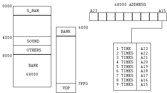
SETTING METHOD
When accessing to the 68000 side addresses from Z80 side, all the addresses can be classified into BANKs. BANK can be set by writing 9 times in 0 bit of 8000 (Z80 Address). The 9 bits correspond to 68000 address 15 - 23 as shown below:
5. VRAM MAPPING
In VRAM, there are various TABLEs and PATTERN GENERATORs as stated below. Among those, the base address of PATTERN GENERATOR TABLE and SPRITE GENERATOR TABLE are 0000H and fixed. However, the other base addresses can be freely assigned in VRAM by setting VDP REGISTER. Also, AREA can be overlapped. Therefore, TABLE can be commonly used by SCROLL screen and WINDOW for example.
SCROLL A PATTERN NAME TABLE Max. 8K Byte.
Base address designated by Register #2.
SCROLL B PATTERN NAME TABLE Max. 8K Byte.
Base address designated by REGISTER #4.
WINDOW PATTERN NAME TABLE varies by H Resolution
Base address designated by REGISTER #3.
H SCROLL DATA TABLE 1K Byte
Base address designated by REGISTER #13
SPRITE ATTRIBUTE TABLE Varies by H Resolution
Base address designated by REGISTER #5
PATTERN GENERATOR TABLE
Base address is 0000H (fixed).
SPRITE GENERATOR TABLE
Base address is 0000H (fixed).
There are 1K Bytes for H SCROLL TABLE, however, as for display 896 Bytes in V28 cell mode and 980 bytes in V30 cell mode. There are 2K bytes for WINDOW PATTERN NAME TABLE in H32 cell mode, and 4K byte area in H 40 cell mode. For details refer to WINDOW. There are 512 bytes for SPRITE ATTRIBUTE TABLE in H32 cell and 1K byte area in H40 cell mode. However as for display, there are 640 bytes in H40 cell mode.
Setting example
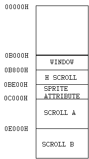
1 H 32 cell mode
SCROLL A PATTERN NAME TABLE
8K Bytes from 0C000H : REG. #2 = $30
SCROLL B PATTERN NAME TABLE
8K Bytes from 0E000H : REG. #4 = $07
WINDOW PATTERN NAME TABLE
2K Bytes from 0B000H : REG. #3 = $2C
H SCROLL DATA TABLE
1K Bytes from 0B800H : REG. #13= $2E
SPRITE ATTRIBUTE TABLE
512 Bytes from 0BE00H : REG. #5 = $5F
Unoccupied area is used as PATTERN GENERATOR and SPRITE GENERATOR.
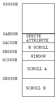
2 H40 cell mode
SCROLL A PATTERN NAME TABLE
8K Bytes from 0C000H : REG. #2 = $30
SCROLL B PATTERN NAME TABLE
8K Bytes from 0E000H : REG. #4 = $07
WINDOW PATTERN NAME TABLE
4K Bytes from 0B000H : REG. #3 = $2C
H SCROLL DATA TABLE
2K Bytes from 0AC00H : REG. #13= $2B
SPRITE ATTRIBUTE TABLE
1K Bytes from 0A800H : REG. #5 = $54
Unoccupied area is used as PATTERN GENERATOR and SPRITE GENERATOR.
PRECAUTIONS FOR MS (MASTER SYSTEM) SOFTWARE PROGRAMMING
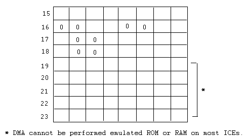
When programming the MS software, pay attention to the following:
1. The program of DMA (RAM, ROM-VRAM, CRAM, VSRAM) should be resident in RAM, or it should be as in LIST1 for example. However, in either one on the above 2 cases, a long word access is not possible as regards the last VRAM address set.
2. ID should be as in the next page.
3. Put LIST2 at your program's start. This is the U.S. security software.
LIST1
DMA_RAM:
         lea     vdp_cmd,An             ; vdp_cmd: $C00000
                                        ; An = ADDRESS REGISTER
         ; Set source ADDRESS to VDP REGISTER
         ; Set DATA LENGTH to VDP REGISTER
         move.l xx,ram0                 ; xx: DESTINATION ADDRESS
                                        ; ram0 :WORK RAM
         move.w ram0,(An)
         move.w ram0+2,(An)             ; Pay careful attention to the
                                        ; sequential order of 1st
                                        ; word and 2nd word.
         rts                            ; DESTINATION ADDRESS should be set
                                        ; by WORD and not by LONG WORD.
LIST 2
         move.b $A10001,d0             ; Get version number
         andi.b #$0F,d0                ;
         beq.b ?0                      ; If not version $0
         move.l $'SEGA',$A14000        ; Output ASCII
?0:
ROM CARTRIDGE DATA FOR MEGA DRIVE
Write in ROM's 100H-1FFH.
100H: 'SEGA MEGA DRIVE ' | 1
| 110H: '(C)SEGA 1988.JUL' | 2
| 120H: GAME NAME (DOMESTIC) | 3
| 150H: GAME NAME (OVERSEAS) | 4
| 180H: 'GM XXXXXXX-XX' | 5
| 18EH: $XXXX | 6
| 190H: CONTROL DATA | 7
| 1A0H: $000000, $XXXXXX | 8
| 1A8H: $FF0000, $FFFFFF | 9
| 1B0H: EXTERNAL RAM DATA | 10
| 1BCH: MODEM DATA | 11
| 1C8H: MEMO | 12
| 1F0H: Country in which the product can be released. | 13
| |
1: SEGA system name and TITLE in common with all ROMs.
2: Copyright notice and year/month of release (Firm name in ASCII 4 character.)
3: Game name for Domestic (JIS KANJI CODE OK)
4: Game name for overseas market (JIS KANJI CODE OK)
5: Type of CARTRIDGE and Products, No., Version No.
TYPE GAME : GM
EDUCATION: Al
NO. PRODUCT NO.
VER. Data varies depending on the type of ROM or software version.
6: Check sum
7: I/0 use support data
JOYSTICK FOR MS: 0 TABLET : T
JOYSTICK : J CONTROL BALL : B
KEYBOARD : K PADDLE CONTROLLER : V
SERIAL (RS232C): R FDD : F
PRINTER : P CDROM : C
8: ROM capacity START ADDRESS, END ADDRESS
9: RAM capacity START ADDRESS, END ADDRESS
10: When no external RAM is mounted, fill the address by a space code and when it is mounted follow the following:
1 B 0 H: dc.b 'RA',%1x1yz000,%00100000
x1 for BACKUP and 0 If not BACKUP
y z10 if even address only. 11 if odd address only
00 if both even and odd address
1 B 4 H: dc.l RAM start address RAM end address
11: If corresponding to MODEM, fill it by space code and if not, follow the following: 1 B C H: dc.b 'MO','xxxx','yy.z'
xxxx Firm name the same as in 2
yy MODEM NO.
z Version
13: Data of the countries in which the product can be released.
JAPAN : J
USA : U
EUROPE : E
Be sure to input a space code in the unoccupied 1 ~ 7, 9 ~ 13 space.
HOW TO OBTAIN CHECK SUM
The CHECK SUM obtaining program is shown as follows. The program starts with 0FF8000H, RAM space. First. fill game capacity by -1 (0FFH) and then load all of the programs. Next, load the CHECK SUM program and run the program from 0FF8000H. After a while, stop running the program. At this time, the lower WORD of DATA REGISTER 0 (d0) is the CHECK SUM value. Note that BREAK in MEMORY should be canceled in advance.
Also, when burning to ROM, first fill the game capacity by -1 (0FFH).
end_addr equ     $1A4
         org     -$8000
start:
         move.l   (a0),d1
         addq.l   #$1,d1
         movea.l  #$200,a0
         sub.l    a0,d1
         amr.l    s1,d1        ; counter
         move     d1,d2
         subq.w   #$1,d2
         swap     d1
         moveq    #$0,d0
?l2:
         add      (a0)+,d0
         dbra     d2,?l2
         dbra     d1,?l2
         nop
         nop
         nop
         nop
         nop
         nop
?le:
         nop
         nop
         bra.b    ?le
MEMORY MAPPING FOR EMULATION
For the 68000 EMULATION
All address should be disabled initially: 0 to 0FFFFFF
Required areas should then be enabled as follows:
1. Program and Data are in 0 to 007FFFF
2. S-RAM is for Z-80 in 0A00000 to 0A01FFF
3. FM sound chip interface is in 0A04000 to 0A04FFF
4. I/O and Z-80 control port are in 0A10000 to 0A11FFF
5. VDP and sound control port are in 0C00000 to 0C00FFF
6. Scratch RAM is in 0FF0000 to 0FFFFFF
RAM CARD (No. 171-5642-02)
This board has two memory areas;
MAIN MEMORY (D-RAM) $000000 - $0FFFFF
BACK UP MEMORY (S-RAM) $200000 - $203FFF
I. INITIALIZE
Write 0100H into $0A11000
Write1 into $0A130F0
(Green LED light up)
2. WRITE PROTECT
Write 3 into $0A130F0
(Red LED light up)
3. READ/WRITE
Write 1 into $0A130F0
(Red LED turns off)
4. NOTE - Emulator access to these ports should be enabled before the writes, then disabled after words.
GENESIS SOUND
SOFTWARE MANUAL
INDEX
I. Z80 MAPPING
(1) Z80 MEMORY MAP
(2) INTERRUPT
II. 68K CONTROL OF Z-80
(1) Z80 START UP
(2) Z80 HANDSHAKE
III. FM SOUND CONTROL
(1) 68K ACCESS FM CHIP
(2) Z80 ACCESS FM CHIP
IV. PSG CONTROL
V.D/A CONTROL
This manual explains memory mapping and way of accessing especially. FM sound generation and PSG are explained another manual.
I. Z80 MAPPING
(2) Z80 MAP
We show the memory at right. I/O is contained in memory map.
1) PROGRAM AREA
Program, data and scratch are in 0 to 1FFFH, is S-RAM.
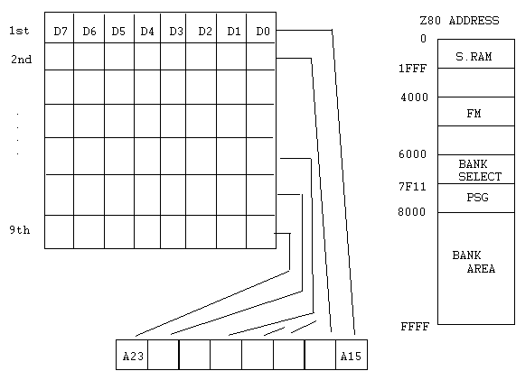
2) BANK
From 8000H - FFFFH is window of 68K memory.
Z-80 can access all of 68K memory by BANK switching. BANK select data create 68K address from A15 to A23. You must write these 9 bits one at a time into 6000H serially, byte units, using the LSB.
3)I/O
4000H FM1 register select (Channel 1-3)
4001H FM1 DATA
4002H FM2 register select (Channel 4-6)
4003H FM2 DATA
PSG address is in 7F11H.
(2) INTERRUPT
Z-80 gets the only VIDEO vertical interrupt. This interrupt is generated 16ms period and 64ms length.
II. 68K CONTROL OF Z80
(1) Z80 START UP
Z-80 OPERATION SEQUENCE.
(1) BUS REQ ON
(2) BUS RESET OFF
(3) 68K copies program into Z-80 S-RAM
(4) BUS RESET ON
(5) BUS REQ OFF
(6) BUS RESET OFF
BUS REQUEST
BUS REQ ON
DATA 100H (WORD) -> $A11100
BUS REQ OFF
DATA OH (WORD) -> $A11100
RESET Z-80
• RESET ON
DATA OH (Word) -> $A11200
• RESET OFF
DATA 100H (Word) -> $A11200
This period requires 26ms.
Also FM sound source is cleared at the same time.
CONFIRMATION OF BUS STATUS
This information is in $A11100 bit 0
0 - Z80 is using
1 - 68K can access
(2) Z80 HANDSHAKE
If you access the Handshake area (A00000 - A07FFF) you must use BUS REQ. 68K has to access the Z-80 S-RAM by byte.
III. FM SOUND CONTROL
(1) 68K accesses the FM source. 68K needs BUS REQ when accessing the FM source, because this memory is controlled by Z-80.
(2) Z80 accesses the FM source.
Z80 normally controls the FM (4000H - 4003H)
IV. PSG CONTROL
PSG accepts access of 68K and Z80 anytime, but you have to coordinate 68K and Z80 accesses.
PSG is in $C00011 from 68K and in 7F11H from Z80.
OVERVIEW
The Yamaha 2612 Frequency Modulation (FM) sound synthesis IC resembles the Yamaha 2151 (used in Sega's coin-op machines) and the chips used in Yamaha's synthesizers.
Its capabilities include:
-- 6 channels of FM sound
-- An 8-bit Digitized Audio channel (as replacement for one of the
FM channels) -- Stereo output capability
-- One LFO (low frequency oscillator) to distort the FM sounds
-- 2 timers. for use by software
To define these terms more carefully; an FM channel is capable of expressing, with a high degree of realism, a single note in almost any instrument's voice. Chords are generally created by using multiple FM channels.
The standard FM channels each have a single overall frequency and data for how to turn this frequency into the complex final wave form (the voice). This conversion process uses four dedicated channel components called 'operators', each possessing a frequency (a variant of the overall frequency), an envelope, and the capability to modulate its input using the frequency and envelope. The operator frequencies are offsets of integral multiples of the overall frequency.
There are two sets of three FM channels, named channels 1 to 3 and 4 to 6 respectively. Channels 3 and 6, the last in each set, have the capability to use a totally separate frequency for each operator rather than offsets of integral multiples. This works well (I believe) for percussion instruments, which have harmonics at odd multiples such as 1.4 or 1.7 of the fundamental.
The 8-bit Digitized Audio exists as a replacement of FM channel 6, meaning that turning on the DAC turns off FM channel 6. Unfortunately, all timing must be done by software -- meaning that unless the software has been very cleverly constructed, it is impossible to use any of the FH channels at the same time as the DAC.
Page 2
Stereo output capability means that any of the sounds. FM or DAC, may be directed to the left, the right, or both outputs. The stereo is output only through the headphone jack.
The LFO, or Low Frequency Oscillator, allows for amplitude and/or frequency distortions of the FM sounds. Each channel elects the degree to which it will be distorted by the LFO, if at all. This could be used, for example, in a guitar solo.
Finally, the system has two software timers, which may be used as an alternative to the Z80 VBLANK interrupt. Unfortunately, these timers do not cause interrupts -- they must be read by the software to determine if they have finished counting.
A LITTLE BIT ABOUT OPERATORS
There are four dedicated operators assigned to every channel, with the following properties:
-- An operator has an input, a frequency and envelope with. which to modify the input, and an output.
-- The operators have two types, those whose outputs feed into another operator, and those that are summed to form the final wave form. The latter are called 'slots'.
-- The slots may be independently enabled, though Sega's software always enables or disables them all simultaneously.
-- Operator 1 may feed back into itself, resulting in a more complex wave form.
These operators may be arranged in eight different configurations, called "algorithms". A diagram of the algorithms follows on the next page.
Page 3
Algorithm 0 -- distortion guitar, "high hat chopper" (?) bass
Algorithm 1 -- harp, PSG (programmable sound generator) sound
Algorithm 2 -- bass, electric guitar, brass, piano, woods
Algorithm 3 -- strings, folk guitar, chimes
Algorithm 4 -- flute, bells, chorus, bass drum, snare drum, tom-tom
Algorithm 5 -- brass, organ
Algorithm 6 -- xylophone, tom-tom, organ, vibraphone
-- snare drum, base drum
Algorithm 7 -- pipe organ
Page 4
REGISTER OVERVIEW
The system is controlled by means of a large number of registers. General system registers are:
-- timer values and status, software use
-- LFO enable and frequency. to distort the FM channels
-- DAC enable and amplitude
-- output enables for each of the 6 FM channels
-- number of frequencies to be used in FM channels 3 and 6 Usually, an FM channel has only one overall frequency, but if so elected, FM channels 3 and 6 use four separate frequencies, one for each operator.
The remainder of the registers apply to a single FM channel, or to an operator in that channel. Registers that refer to the channel as a whole are:
-- frequency number (in the standard case) -- algorithm number
-- extent of self-feedback in operator 1
-- output type, to L, R, or both speakers. This can only be heard if headphones are used.
-- the extent to which the channel is distorted by the LFO.
Registers that refer to each operator make up the remainder. The four operator's connections are determined by the algorithm used, but the envelope is always specified individually for each operator. In the case of FM channels 3 and 6, the frequency may be specified individually for each operator.
Page 5
ENVELOPE SPECIFICATION
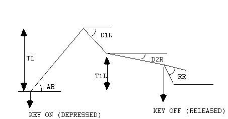
The sound starts when the key is depressed, a process called 'key on'. The sound has an attack, a strong primary decay, followed by a slow secondary decay. The sound continues this secondary decay until the key is released, a process called 'key off'. The sound then begins a rapid final decay, representing for example a piano note after the key has been released and the damper has come down on the strings.
The envelope is represented by the above amplitudes and angles, and a few supplementary registers. Used in the above diagram are:
TL -- Total level, the highest amplitude of the wave form
AR -- Attack rate, the angle of initial amplitude increase. This can be made very steep if desired. The problem with slow attack rates is that if the notes are short, the release (called 'key off') occurs before the note has reached a reasonable level.
D1R -- The angle of initial amplitude decrease
T1L --. The amplitude at which the slower amplitude decrease starts
D2R -- The angle of secondary amplitude decrease. This will continue indefinitely unless 'key off' occurs.
RR -- The final angle of amplitude decrease, after 'key off'.
Page 5 1/2
Additional registers are:
RS -- Rate scaling. The degree to which envelopes become shorter as frequencies become higher. For example, high notes on a piano fade much more quickly than low notes.
AM -- Amplitude Modulation enable, whether or not this operator will allow itself to be modified by the LFO. Changing the amplitude of the slots (those colored gray in the diagram on page 3) changes the loudness of the note; changing the amplitude of the other operators changes its flavor.
SSG-EG -- a proprietary register whose usage is unknown. It should be set to 0.
Page 6
The FM-2612 may be accessed from either the 68000 or the Z80. In both cases, however, the bus is only 8 bits wide.
The FM-2612 is accessed through memory locations 4000H - 4003H in the Z80 case, or A04000H - A04003H in the 68000 case. These will be referred to as 4000 to 4003.
The internal registers of the FM-2612 are divided as follows;

Page 7
To units to Part I, write the 8 bit address to 4000 and the data to 4001. To write to PART II, write the 8-bit address to 4002 and the data to 4003.
CAUTION: Before writing, read from any address to determine if the YM-2612 I/O is still busy from the last write. Delay until bit 7 returns to 0.
CAUTION: in the case of registers that are "ganged together" to form a longer number - for example the 10-bit Timer A value or the 14-bit frequencies, write the high register first.
READ DATA: Reading from any of the four locations.
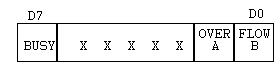
BUSY - 1 if busy, 0 if ready for new data
OVERFLOW - 1 if the timer has counted up and overflowed. See register 27H.
Page 8
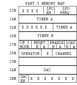
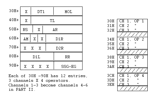
Page 9
PART I MEMORY MAP (Cont.)
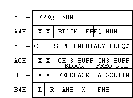
Each of the above has three entries. All follow the pattern:

with the exception that A8H and ACH follow the pattern:

"PART II" is a duplication of 30H - B4H, where channels 1-3 are replaced by 4-6.
Page 10
The Registers:

LFO EN - 1 is enabled, 0 is disabled.
LFO FREQ.
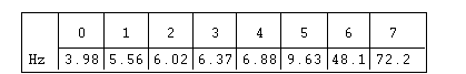
The LFO (Low frequency Oscillator) is used to distort the FM sounds amplitude and phase. It is triple enabled, as there is:
A) A global enable in Reg. 22H
B) A sensitivity enable on a channel by channel basis, in Regs. 60H - 6EH.
If the LFP is desired, enable it by register 22H. Next, select which channels will be affected by the LFO, to what degree, and whether their amplitude or phase ___ ___ ___.
Page 11
affected, by setting registers B4 - B6H. Finally. if a channel's amplitude is affected, make sure that it is only the "slots" that are affected by setting registers 60H - 6EH.


Registers 24H and 25H are ganged together to form 10-bit TIMER A, with register 25H containing the least significant bits. They should be set in the order 24H, 25H. The timer lasts:
18 * (1024 - TIMER A) microseconds
Timer A - all 1's -> 18 µs = 0.018 ms
Timer A - all 0's -> 18,400 µs = 18.4 ms
Page 12

8 Bit Timer B lasts
288 * (256 - TIMER B ) microseconds
TIMER B = all 1's -> 0.288 ms
TIMER B = all 0's -> 73.44 ms
Register 27H controls the software timers and the Channel 3 (and 6) mode, two entirely separate items.
| CH 3 MODE | D7 D6 | |
| NORMAL | 0 0 | Channel 3 is the same as the others |
| SPECIAL | 0 1 | Channel 3 has 4 separate frequencies |
| ILLEGAL | 1 X | — |
Page 13
A normal channel's operators use offsets of integral multiples of a single frequency. In special mode, each operator has an entirely separate frequency. Channel 3 operator 1's frequency is in registers A2 and A6. Operators 2 to 4 are in Regs. A8 and AC, A9 and AD, and AA and AE respectively.
No one at Sega has used the timer feature, but the Japanese manual says;
LOAD - 1 starts the timer, 0 stops it.
ENABLE - 1 causes timer overflow to set the read register flag. 0 means the timer keeps cycling without setting the flag.
RESET - Writing a 1 clears the read register flag, writing a 0 has no effect.
Page 14

This register is used for "Key on" and "Key off". "Key on" is the depression of the synthesizer key. "Key off" is its release. The sequence of operations is; set parameters, Key on, wait, key off. When key off occurs, the FM channel stops its slow decline and starts the rapid decline specified by "RR", the release rate.
In a single write to register 28H, one sets the status of all operators for a single channel. Sega always sets them to the same value, on (1) or off (0). Using a special channel 3, I believe it is possible to have each operator be a separate note, so there is possible justification for turning then on and off separately.
Page 15
![]()
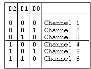

Register 2AH contains 8 bit DAC data.

If the DAC enable is 1, the DAC data is output as a replacement for channel 6. The only Channel 6 register that affects the DAC is the stereo output portion of reg. B4H.
Page 16
Registers 30H - 90H are all single - operator registers. Please see page 8 for how the twelve channel - operator combinations are arranged.

Both DT1 (Detune) and MUL (Multiple) relate the operator's frequency to the overall frequency.
MUL ranges from 0 to 15, and multiples the overall frequency, with the exception that 0 results in multiplication by 1/2. That is, MUL=0 to 15 gives *1/2, *1, *2, ... *15.
DT1 gives small variations from the overall frequency * MUL. The MSB of DT1 is a primitive sign bit, and the two LSB's are magnitude bits. See the next page for a diagram.
Page 17
| D6 D5 D4 | Multiplicative Effect | |
| 0 0 0 | No Change | |
| 0 0 1 | X ( 1 + 1*E ) | |
| 0 1 0 | X ( 1 + 2*E ) | |
| 0 1 1 | X ( 1 + 3*E ) | Where E is a small number. |
| 1 0 0 | No Change | |
| 1 0 1 | X ( 1 + 1*E ) | |
| 1 1 0 | X ( 1 + 2*E ) | |
| 1 1 1 | X ( 1 + 3*E ) |

TL (total level) represents the envelopes highest amplitude, with 0 being the largest and 127 the smallest. A change of one unit is about 0.75 dB. To make a note softer, only change the TL of the slots (the output operators). Changing the other operators will affect the flavor of the note.

Register 50H contains RS (rate scaling) and AR (attack rate). AR is the steepness of the initial amplitude rise, shown on page 4.
RS affects AR, D1R, D2R and RR in the same way. RS is the degree to which the envelope becomes narrower as the frequency becomes higher. The frequency's top five bits (3 octave bits and 2 note bits) are called KC (Key code) in the following rate formulas:
RS=0 -> Final Rate = 2 * Rate + (KC/8)
RS=1 -> Final Rate = 2 * Rate + (KC/4)
RS=2 -> Final Rate = 2 * Rate + (KC/2)
RS=3 -> Final Rate = 2 * Rate + (KC/1)
KC/N is always rounded down.
As rate ranges from 0-31, this means that the RS influence ranges from small (at 0-3) to very large (at 0-31)
Page 19

D1R (First Decay Rate) is the initial steep amplitude decay rate (see page 4). It is, like all rates, 0-31 in value and affected by RS.
AM is the amplitude modulation enable, whether of not this operator will be subject to amplitude modulation by the LFO. This bit is not relevant unless both the LFO is enabled and register B4's AMS (Amplitude modulation sensitivity) is non-zero.

D2R (secondary decay rate) is the long tail off of the sound that continues as long as the key is depressed.
Page 20

D1L is the secondary amplitude reached after the first period of rapid decay. It should be multiplied by 8 if one wishes to compare it to TL. Again as TL, the higher the number, the more attenuated the sound.
RR is the release rate, the final sharp decrease in volume after the key is released. All rates are 5 bit numbers, but there are only four bits available in the register. Thus, for comparison and calculation purposes, these four bits are the MSBs and the LSB is always 1. In other words, double it and add one.

This register is proprietary and should be set to zero.
The final registers relate mostly to a single channel. Each register is tripled; please see the diagram on page 9.
![]()
![]()
![]()
![]()
Channel 1's frequency is in A0 and A4H.
Channel 2's frequency is in A1 and A5H.
Channel 3's frequency is in normal mode
(Please see page 12) is in A2 and A6H.
If Channel 3 is in special mode:
Operator 1's frequency is in A7 and A6H
Operator 2's frequency is in A8 and ACH
Operator 3's frequency is in A9 and ADH
Operator 4's frequency is in AA and AEH
Page 22
The frequency is a 14-bit number that should be set high byte, low byte (e.g. A4H then A0H). The highest 3 bits called the "block", give the octave. The next 10 bits give position in the octave, and a possible 12 - tone sequence is;
| Low | 617 | |
| 653 | ||
| 692 | ||
| 733 | ||
| 777 | ||
| 823 | All numbers in base 10 | |
| 872 | ||
| 924 | ||
| 979 | ||
| 1037 | ||
| 1099 | ||
| High | 1164 |
This sequence should be used inside each octave.
Page 23
![]()
FEEDBACK is the degree to which operator 1 feeds back into itself. In the voice library, self feedback is represented as this:

The ALGORITHM is the type of inter-operator connection used. Please see the list of the eight operators on page 3.
![]()
Register B4H contains stereo output control and LFO sensitivity control.
L - Left Output, 1 is on, 0 is off.
R - Right Output, 1 is on, 0 is off.
NOTE: The stereo may only be heard by headphones.
Page 24
AMS (Amplitude modulation sensitivity) and FMS (Frequency modulation sensitivity) are the degree to which the channel is affected by the LFO. If the LFO is disabled. this register need not be set. Additionally, amplitude modulation is also enabled on an operator - by operator level.
| AMS | 0 | 1 | 2 | 3 |
| dB | 0 | 1.4 | 5.9 | 11.8 |
| FMS | 0 | 1 | 2 | 3 | 4 | 5 | 6 | 7 |
| % of | 0 | ± 3.4 | ± 6.7 | ± 10 | ± 14 | ± 20 | ± 40 | ± 80 |
a halftone
Page 25
TEST PROGRAM
Here's a tested power-on initialization and sample note in the "Grand Piano" voice (Page 27)
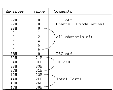
Page 26
| Register | Value | Comments |
| 50H | 5FH | RS/AR |
| 54H | 99H | RS/AR |
| 58H | 5FH | RS/AR |
| 5CH | 94H | RS/AR |
| 60H | 5 | AM/D1R |
| 64H | 5 | AM/D1R |
| 68H | 5 | AM/D1R |
| 6CH | 7 | AM/D1R |
| 70H | 2 | D2R |
| 74H | 2 | D2R |
| 78H | 2 | D2R |
| 7CH | 2 | D2R |
| 80H | 11H | D1L/RR |
| 84H | 11H | D1L/RR |
| 88H | 11H | D1L/RR |
| 8CH | A6H | D1L/RR |
| 90H | 0 | Proprietary |
| 94H | 0 | Proprietary |
| 98H | 0 | Proprietary |
| 9CH | 0 | Proprietary |
| B0H | 32H | FEEDBACK/ALGORITHM |
| B4H | C0H | Both Speakers on |
| 28H | 00H | Key off |
| A4H | 22H | Set Frequency |
| A0H | 69H | Set Frequency |
| 28H | F0H | Key on |
| <Wait> | ||
| 28H | 00H | Key off |
Notes:
#1 Write address then data.
#2 Loop until read register D7 becomes 0
#3 Follow MSB/LSB sequence.
PROGRAMMABLE SOUND GENERATOR (PSG)
The PSG contains four sound channels, consisting of three tone generators and a noise generator. Each of the four channels has an independent volume control (attenuator). The PSG is controlled through output port $7F.
TONE GENERATOR FREQUENCY
The frequency (pitch) of a tone generator is set by a 10-bit value. This value is counted down until it reaches zero, at which time the tone output toggles and the 10-bit value is reloaded into the counter. Thus, higher 10-bit numbers produce lower frequencies.
To load a new frequency value into one of the tone generators, you write a pair of bytes to I/O-location $7F according to the following format:
| First Byte: | 1 | R2 | R1 | R0 | d3 | d2 | d1 | d0 |
| Second Byte: | 0 | 0 | d9 | d8 | d7 | d6 | d5 | d4 |
The R2:R1:R0 field selects the tone channel as follows:
| R2 | R1 | R0 | Tone Chan. |
| 0 | 0 | 0 | #1 |
| 0 | 1 | 0 | #2 |
| 1 | 0 | 0 | #3 |
10-bit data is: (MSB) d9 d8 d7 d6 d5 d4 d3 d2 d1 d0 (LSB)
NOISE GENERATOR CONTROL
The noise generator uses three control bits to select the "character" of the noise sound. A bit called "FB" (Feedback) produces periodic noise or "white" noise:
| FB | Noise Type |
| 0 | Periodic (like low-frequency tone) |
| 1 | White (hiss) |
The frequency of the noise is selected by two bits NF1:NF0 according to the following
| NF1 | NF0 | Noise Generator Clock Source |
| 0 | 0 | Clock/2 [Higher pitch, "less coarse"] |
| 0 | 1 | Clock/4 |
| 1 | 0 | Clock/8 [Lower pitch, "more coarse"] |
| 1 | 1 | Tone Generator #3 |
NOTE: "Clock" is fixed in frequency. It is a crystal controlled oscillator signal connected to the PSG.
When NF1:NF0 is 11, Tone Generator #3 supplies the noise clock source. This allows the noise to be "swept" in frequency. This effect might be used for a jet engine runup, for example. To load these noise generator control bits, write the following byte to I/O port $7F:
| OUT ($7F): | 1 | 1 | 1 | 0 | 0 | FB | NF1 | NF0 |
ATTENUATORS
Four attenuators adjust the volume of the three tone generators and the noise channel. Four bits A3:A2:A1:A0 control the attenuation as follows:
| A3 | A2 | A1 | A0 | Attenuation | |
| 0 | 0 | 0 | 0 | 0 db | (maximum volume) |
| 0 | 0 | 0 | 1 | 2 db | NOTE: a higher attenuation results |
| 0 | 0 | 1 | 0 | 4 db | in a quieter sound. |
| 0 | 0 | 1 | 1 | 6 db | |
| 0 | 1 | 0 | 0 | 8 db | |
| 0 | 1 | 0 | 1 | 10 db | |
| 0 | 1 | 1 | 0 | 12 db | |
| 0 | 1 | 1 | 1 | 14 db | |
| 1 | 0 | 0 | 0 | 16 db | |
| 1 | 0 | 0 | 1 | 18 db | |
| 1 | 0 | 1 | 0 | 20 db | |
| 1 | 0 | 1 | 1 | 22 db | |
| 1 | 1 | 0 | 0 | 24 db | |
| 1 | 1 | 0 | 1 | 26 db | |
| 1 | 1 | 1 | 0 | 28 db | |
| 1 | 1 | 1 | 1 | -Off- |